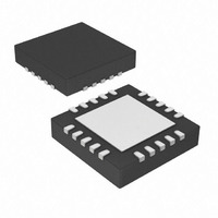
PIC16F785T-I/ML Microchip Technology, PIC16F785T-I/ML Datasheet - Page 75

PIC16F785T-I/ML
Manufacturer Part Number
PIC16F785T-I/ML
Description
3.5 KB Flash, 128 RAM, 18 I/O 20 QFN 4x4mm T/R
Manufacturer
Microchip Technology
Series
PIC® 16Fr
Datasheets
1.PIC16F616T-ISL.pdf
(8 pages)
2.PIC16F785-ISS.pdf
(206 pages)
3.PIC16F785-ISS.pdf
(10 pages)
4.PIC16F785-ISS.pdf
(28 pages)
Specifications of PIC16F785T-I/ML
Core Processor
PIC
Core Size
8-Bit
Speed
20MHz
Peripherals
Brown-out Detect/Reset, POR, PWM, WDT
Number Of I /o
17
Program Memory Size
3.5KB (2K x 14)
Program Memory Type
FLASH
Eeprom Size
256 x 8
Ram Size
128 x 8
Voltage - Supply (vcc/vdd)
2 V ~ 5.5 V
Data Converters
A/D 14x10b
Oscillator Type
Internal
Operating Temperature
-40°C ~ 85°C
Package / Case
20-VQFN Exposed Pad, 20-HVQFN, 20-SQFN, 20-DHVQFN
Lead Free Status / RoHS Status
Lead free / RoHS Compliant
Connectivity
-
Lead Free Status / RoHS Status
Lead free / RoHS Compliant, Lead free / RoHS Compliant
- PIC16F616T-ISL PDF datasheet
- PIC16F785-ISS PDF datasheet #2
- PIC16F785-ISS PDF datasheet #3
- PIC16F785-ISS PDF datasheet #4
- Current page: 75 of 206
- Download datasheet (4Mb)
10.2
The VR Reference module generates a 1.2V nominal
output voltage for use by the ADC and comparators.
The output voltage can also be brought out to the V
pin for user applications. This module uses a bandgap
as a reference. See Table 19-9 for detailed specifica-
tions. Register 10-2 shows the control register for the
VR module.
REGISTER 10-2:
© 2008 Microchip Technology Inc.
bit 7
Legend:
R = Readable bit
-n = Value at POR
bit 7-6
bit 5
bit 4
bit 3
bit 2
bit 1
bit 0
Note 1: Buffer amplifier common mode limitations require V
U-0
—
2: VREN is fixed high for PIC16HV785 device.
VR Reference Module
Unimplemented: Read as ‘0’
BGST: Band Gap Reference Voltage Stable Flag bit
1 = Reference is stable
0 = Reference is not stable
VRBB: Voltage Reference Buffer Bypass bit
1 = V
0 = V
VREN: Voltage Reference Enable bit (VR = 1.2V nominal)
1 = VR reference is enabled
0 = VR reference is disabled and does not consume any current
VROE: Voltage Reference Output Enable bit
If CVROE = 0:
1 = V
0 = Disabled, 1.2 volt VR analog reference is used internally only
If CVROE = 1:
CVROE: Comparator Voltage Reference Output Enable bit (see Figure 10-2)
1 = V
0 = V
Unimplemented: Read as ‘0’
VROE has no effect.
U-0
REF
REF
REF
REF
REF
—
REFCON: VOLTAGE REFERENCE CONTROL REGISTER
output is not buffered. Power is removed from buffer amplifier.
output is buffered
output on RA1/AN1/C12IN0-/V
output on RA1/AN1/C12IN0-/V
output on RA1/AN1/C12IN0-/V
W = Writable bit
‘1’ = Bit is set
BGST
R-0
(1)
R/W-0
VRBB
REF
REF
REF
REF
U = Unimplemented bit, read as ‘0’
‘0’ = Bit is cleared
/ICSPCLK pin is 1.2 volt VR analog reference
/ICSPCLK pin is CV
/ICSPCLK pin is controlled by VROE
R/W-0
VREN
REF
≤ (V
PIC16F785/HV785
DD
(2)
- 1.4)V for buffered output.
R/W-0
VROE
REF
voltage
x = Bit is unknown
CVROE
R/W-0
DS41249E-page 73
U-0
—
bit 0
Related parts for PIC16F785T-I/ML
Image
Part Number
Description
Manufacturer
Datasheet
Request
R

Part Number:
Description:
IC PIC MCU FLASH 2KX14 20SOIC
Manufacturer:
Microchip Technology
Datasheet:

Part Number:
Description:
IC PIC MCU FLASH 2KX14 20QFN
Manufacturer:
Microchip Technology
Datasheet:

Part Number:
Description:
IC PIC MCU FLASH 2KX14 20DIP
Manufacturer:
Microchip Technology
Datasheet:

Part Number:
Description:
IC PIC MCU FLASH 2KX14 20SSOP
Manufacturer:
Microchip Technology
Datasheet:

Part Number:
Description:
IC PIC MCU FLASH 2KX14 20SOIC
Manufacturer:
Microchip Technology
Datasheet:

Part Number:
Description:
IC PIC MCU FLASH 2KX14 20DIP
Manufacturer:
Microchip Technology
Datasheet:

Part Number:
Description:
3.5 KB Flash, 128 RAM, 18 I/O 20 QFN 4x4mm TUBE
Manufacturer:
Microchip Technology
Datasheet:

Part Number:
Description:
20 PIN, 3.5 KB STD FLASH, 128 RAM, 18 I/O PB FREE,
Manufacturer:
Microchip Technology
Datasheet:

Part Number:
Description:
IC, 8BIT MCU, PIC16F, 32MHZ, SOIC-18
Manufacturer:
Microchip Technology
Datasheet:

Part Number:
Description:
IC, 8BIT MCU, PIC16F, 32MHZ, SSOP-20
Manufacturer:
Microchip Technology
Datasheet:

Part Number:
Description:
IC, 8BIT MCU, PIC16F, 32MHZ, DIP-18
Manufacturer:
Microchip Technology
Datasheet:

Part Number:
Description:
IC, 8BIT MCU, PIC16F, 32MHZ, QFN-28
Manufacturer:
Microchip Technology
Datasheet:

Part Number:
Description:
IC, 8BIT MCU, PIC16F, 32MHZ, QFN-28
Manufacturer:
Microchip Technology
Datasheet:

Part Number:
Description:
IC, 8BIT MCU, PIC16F, 32MHZ, QFN-28
Manufacturer:
Microchip Technology
Datasheet:

Part Number:
Description:
IC, 8BIT MCU, PIC16F, 32MHZ, SSOP-20
Manufacturer:
Microchip Technology
Datasheet:


