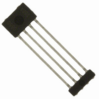
A1354KKT-T Allegro Microsystems Inc, A1354KKT-T Datasheet

A1354KKT-T
Specifications of A1354KKT-T
Related parts for A1354KKT-T
A1354KKT-T Summary of contents
Page 1
High Precision 2-Wire Linear Hall Effect Sensor IC Features and Benefits ▪ Designed for automotive, battery-powered applications ▪ Customer programmable quiescent duty cycle, sensitivity, and PWM carrier frequency, through VCC pin ▪ Simultaneous programming of duty cycle, sensitivity, and PWM ...
Page 2
... Features and Benefits (continued) ▪ Output duty cycle clamps provide short circuit diagnostic capabilities ▪ Optional 50% duty cycle calibration test mode at device power-up Selection Guide Part Number A1354KKTTN-T 4000 pieces per 13-in. reel ® *Contact Allegro for additional packing options Absolute Maximum Ratings ...
Page 3
A1354 OPERATING CHARACTERISTICS (A) noted Characteristics ELECTRICAL CHARACTERISTICS Supply Voltage 2 Supply Current Supply Current Ratio 3 4 Power-On Time Supply Zener Clamp Voltage Internal Bandwidth Chopping Frequency 5 OUTPUT CHARACTERISTICS Response Time 4 6 Clamp Duty Cycles 4,7 Duty ...
Page 4
A1354 PROGRAMMING CHARACTERISTICS Characteristics 2 PRE-PROGRAMMING TARGET Pre-Programming Quiescent Duty Cycle Output Pre-Programming Sensitivity Pre-Programming PWM Output Carrier Frequency QUIESCENT DUTY CYCLE PROGRAMMING 3 Initial Quiescent Duty Cycle Output Guaranteed Quiescent Duty Cycle Programming Range 4 Quiescent Duty Cycle Output ...
Page 5
A1354 PROGRAMMING CHARACTERISTICS (continued) Characteristics CALIBRATION TEST MODE PROGRAMMING Calibration Test Mode Selection Bit LOCK BIT PROGRAMMING Overall Programming Lock Bit (gauss) = 0.1 mT (millitesla). 2 Raw device characteristic values before any programming may ...
Page 6
A1354 OPERATING CHARACTERISTICS (B) otherwise noted Characteristics FACTORY PROGRAMMED SENSITIVITY TEMPERATURE COEFFICIENT AND SENSITIVITY DRIFT Sensitivity Temperature Coefficient 1 Maximum Sensitivity Drift Through Temperature Range 2,3 Sensitivity Drift Due to Package 3,4 Hysteresis FACTORY PROGRAMMED DUTY CYCLE DRIFT 1,3 Duty ...
Page 7
A1354 Thermal Characteristics may require derating at maximum conditions Characteristic Package Thermal Resistance *Additional thermal information available on Allegro website. High Precision 2-Wire Linear Hall Effect Sensor IC with Pulse Width Modulated Output Symbol 1-layer PCB with copper limited to ...
Page 8
A1354 ≈10% Duty Cycle (Low Clamp) ≈ 50% Duty Cycle ≈ 90% Duty Cycle (High Clamp) High Precision 2-Wire Linear Hall Effect Sensor IC with Pulse Width Modulated Output V at Various Duty Cycles CC 4 μs per division T ...
Page 9
A1354 Quiescent Voltage Output and Duty Cycle The operating output voltage determined by the PWM output voltage OUT duty cycle turn proportional to a change in air gap between the A1354 Hall element ...
Page 10
A1354 and for unipolar devices as: D – D (BPOS) (Q) Sens = BPOS where BPOS and BNEG are two magnetic fields with opposite polarities. Guaranteed Sensitivity Range The magnetic sensitivity, Sens, can be programmed around its nominal value within ...
Page 11
A1354 Linearity Error is calculated separately for the positive (Lin ) and negative (Lin ERRPOS ERRNEG Linearity error (%) is measured and defined as: D – (+B) Lin – ERRPOS = D (+B½) – D ...
Page 12
A1354 BYPASS 0.01 μF When using Hall-effect technology, a limiting factor for switchpoint accuracy is the small signal voltage developed across the Hall element. This voltage is disproportionally small relative to the offset that can be produced ...
Page 13
A1354 Overview Programming is accomplished by sending a series of input voltage pulses serially through the VCC pin of the device. Unique combi- nations of different voltage amplitude pulses control the internal programming logic of the device to select a ...
Page 14
A1354 Mode and Parameter Register Selection Each mode and programmable parameter can be accessed through a specific register. To select a register, a sequence of voltage pulses consisting of a VPH pulse, a series of VPM pulses, and a VPH ...
Page 15
A1354 in figure 5. The order of blowing bits, however, is not important. Blowing bit 0 first, and then bit 2 is acceptable. Note: After blowing, the programming is not reversible, even after cycling the supply power. Although a register ...
Page 16
A1354 Programming Modes Try Mode This mode allows multiple programmable parameters to be tested simultaneously without permanently setting any values. In this mode, each VPH pulse will indefinitely loop the programming logic through the Mode Select, Register Select, and Bitfield ...
Page 17
A1354 Power-up User Power-down Required Fuse Blowing Yes Initial State A known state to which the programming logic is reset after system power-up. All the bitfield locations that have intact fuses are reset to logic 0. VPM pulses have no ...
Page 18
A1354 Programming Logic Register Selection Key Binary Format (MSB → LSB) Blow / Lock 1 Try 2 Sensitivity / Coarse D (Q) 000000000 011111111 1 1 00000000 Fine gauss) (Q) 000000000 011111111 2 1 00000000 111111111 ...
Page 19
A1354 This example demonstrates the programming of the device. The recommended sequence for programming is shown in the Addi- tional Guidelines section, but for this example, we start at setting the register for Fine Duty Cycle and then go on ...
Page 20
A1354 The Calibration Test mode is provided so that the user can com- pensate for differences in the ground potential between the A1354 and any interface circuitry used to measure the pulse width of the A1354 output. This test mode ...
Page 21
A1354 device output waveform is a fixed 50% duty cycle (the pro- grammed quiescent duty cycle value) regardless of the applied external magnetic field. After powering-up, the A1354 outputs its quiescent duty cycle waveform for 800 ms, regardless of the ...
Page 22
A1354 5.21 10° +0.08 3.43 –0.05 0.89 MAX 12.14±0.05 +0.08 0.41 –0.05 0.89 MAX 1 2 +0.08 1.50 –0.05 5.21 Copyright ©2009, Allegro MicroSystems, Inc. The products described herein are manufactured under one or more of the following U.S. patents: ...


