ADIS16405BMLZ Analog Devices Inc, ADIS16405BMLZ Datasheet - Page 4
ADIS16405BMLZ
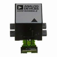
Manufacturer Part Number
ADIS16405BMLZ
Description
MODULE GYRO/ACCEL/MAG 24ML
Manufacturer
Analog Devices Inc
Specifications of ADIS16405BMLZ
No. Of Axes
3
Sensor Case Style
ML-24-2
No. Of Pins
24
Supply Voltage Range
4.75V To 5.25V
Operating Temperature Range
-40°C To +105°C
Termination Type
Through Hole
Acceleration Range
2000g
Interface Type
SPI
Sensitivity Per Axis
3.33mg / LSB
Rohs Compliant
Yes
Filter Terminals
Through Hole
Digital Ic Case Style
Module
Lead Free Status / RoHS Status
Lead free / RoHS Compliant
For Use With
ADIS16405/PCBZ - BOARD EVAL FOR ADIS16405
Lead Free Status / RoHS Status
Lead free / RoHS Compliant, Lead free / RoHS Compliant
Available stocks
Company
Part Number
Manufacturer
Quantity
Price
Company:

Part Number:
ADIS16405BMLZ
Manufacturer:
AD
Quantity:
4
Part Number:
ADIS16405BMLZ
Manufacturer:
ADI/亚德诺
Quantity:
20 000


ADIS16405
Parameter
ADC INPUT
DAC OUTPUT
LOGIC INPUTS
DIGITAL OUTPUTS
FLASH MEMORY
FUNCTIONAL TIMES
CONVERSION RATE
POWER SUPPLY
1
2
3
4
The digital I/O signals are driven by an internal 3.3 V supply, and the inputs are 5 V tolerant.
Endurance is qualified as per JEDEC Standard 22, Method A117, and measured at −40°C, +25°C, +85°C, and +125°C.
The data retention lifetime equivalent is at a junction temperature (T
temperature.
These times do not include thermal settling and internal filter response times (330 Hz bandwidth), which may affect overall accuracy.
Resolution
Integral Nonlinearity
Differential Nonlinearity
Offset Error
Gain Error
Input Range
Input Capacitance
Resolution
Relative Accuracy
Differential Nonlinearity
Offset Error
Gain Error
Output Range
Output Impedance
Output Settling Time
Input High Voltage, V
Input Low Voltage, V
CS Wake-Up Pulse Width
Logic 1 Input Current, I
Logic 0 Input Current, I
Input Capacitance, C
Output High Voltage, V
Output Low Voltage, V
Data Retention
Power-On Start-Up Time
Reset Recovery Time
Sleep Mode Recovery Time
Flash Memory Test Time
Automatic Self-Test Time
Clock Accuracy
Sync Input Clock
Operating Voltage Range, VCC
Power Supply Current
All Pins Except RST
RST Pin
1
3
1
4
IN
INL
INH
OL
INH
INL
OH
Test Conditions
During acquisition
Code 101 to Code 4095, 5 kΩ/100 pF to GND
5 kΩ/100 pF to GND
CS signal to wake up from sleep mode
V
V
I
I
Endurance
T
Time until data is available
Normal mode, SMPL_PRD ≤ 0x09
Low power mode, SMPL_PRD ≥ 0x0A
Normal mode, SMPL_PRD ≤ 0x09
Low power mode, SMPL_PRD ≥ 0x0A
Normal mode, SMPL_PRD ≤ 0x09
Low power mode, SMPL_PRD ≥ 0x0A
Normal mode, SMPL_PRD ≤ 0x09
Low power mode, SMPL_PRD ≥ 0x0A
SMPL_PRD = 0x01
SMPL_PRD = 0x01 to 0xFF
Low power mode at 25°C
Normal mode at 25°C
Sleep mode at 25°C
SOURCE
SINK
J
IH
IL
= 85°C
= 0 V
= 3.3 V
= 1.6 mA
= 1.6 mA
2
J
) of 85°C as per JEDEC Standard 22, Method A117. Data retention lifetime decreases with junction
Rev. 0 | Page 4 of 16
Min
0
0
2.0
20
2.4
10,000
10
0.413
4.75
Typ
12
±2
±1
±4
±2
20
12
±4
±1
±5
±0.5
2
10
±0.2
−40
−1
10
220
290
100
170
4
15
17
90
12
5.0
45
70
600
Max
3.3
3.3
0.8
0.55
±10
−60
0.4
819.2
±3
1.2
5.25
Unit
Bits
LSB
LSB
LSB
LSB
V
pF
Bits
LSB
LSB
mV
%
V
Ω
μs
V
V
V
μs
μA
μA
mA
pF
V
V
Cycles
Years
ms
ms
ms
ms
ms
ms
ms
ms
SPS
%
kHz
V
mA
mA
μA
Related parts for ADIS16405BMLZ
Image
Part Number
Description
Manufacturer
Datasheet
Request
R

Part Number:
Description:
±1.7g Dual-Axis IMEMS Accelerometer Evaluation Board
Manufacturer:
Analog Devices Inc
Datasheet:

Part Number:
Description:
Inertial Sensor Evaluation System
Manufacturer:
Analog Devices Inc
Datasheet:
Part Number:
Description:
Manufacturer:
Analog Devices Inc
Datasheet:
Part Number:
Description:
Manufacturer:
Analog Devices Inc
Datasheet:
Part Number:
Description:
Manufacturer:
Analog Devices Inc
Datasheet:
Part Number:
Description:
Manufacturer:
Analog Devices Inc
Datasheet:
Part Number:
Description:
Manufacturer:
Analog Devices Inc
Datasheet:
Part Number:
Description:
Manufacturer:
Analog Devices Inc
Datasheet:
Part Number:
Description:
Manufacturer:
Analog Devices Inc
Datasheet:
Part Number:
Description:
Manufacturer:
Analog Devices Inc
Datasheet:
Part Number:
Description:
Manufacturer:
Analog Devices Inc
Datasheet:
Part Number:
Description:
Manufacturer:
Analog Devices Inc
Datasheet:
Part Number:
Description:
Manufacturer:
Analog Devices Inc
Datasheet: