TC6501P120VCTTRG Microchip Technology, TC6501P120VCTTRG Datasheet - Page 3
TC6501P120VCTTRG
Manufacturer Part Number
TC6501P120VCTTRG
Description
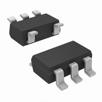
IC TEMP SWTCH OPEN DRAIN SOT23-5
Manufacturer
Microchip Technology
Specifications of TC6501P120VCTTRG
Sensing Temperature
120°C Trip Point
Output Type
Active Low/Open Drain
Voltage - Supply
2.7 V ~ 5.5 V
Accuracy
±0.5°C
Package / Case
SC-74A, SOT-753
Temperature Threshold
+ 120 C
Full Temp Accuracy
6 C
Supply Voltage (max)
5.5 V
Supply Voltage (min)
2.7 V
Maximum Operating Temperature
+ 135 C
Minimum Operating Temperature
- 55 C
Supply Current
40 uA
Lead Free Status / RoHS Status
Lead free / RoHS Compliant
Other names
TC6501P120VCTTRG
TC6501P120VTR
TC6501P120VTR


1.0
Absolute Maximum Ratings†
Input Voltage (V
Output Voltage (OUT to GND) ................................. 6V
Voltage On Any Pin ....... (GND – 0.3V) to (V
Operating Temperature Range ......... –40 C to +125 C
Storage Temperature ........................ –65 C to +150 C
DC CHARACTERISTICS
2004 Microchip Technology Inc.
Electrical Specifications: Unless otherwise specified, V
Supply Voltage
Supply Current
SHDN Input
SHDN Input High Threshold
SHDN Input Low Threshold
PWM Output
PWM Output Low Voltage
PWM Output High Voltage
PWM Rise Time
PWM Fall Time
PWM Frequency
Start-up Time
Temperature Accuracy
High Temperature Accuracy
Temperature Range Accuracy (T
Auto-shutdown Hysteresis
T
T
T
Absolute Accuracy
Trip Point Hysteresis
Note 1:
OVER
OVER
OVER
Output
Output High Voltage
Output Low Voltage
ELECTRICAL
CHARACTERISTICS
Parameters
Transition from 90% to 100% Duty Cycle.
DD
to GND) ................................... +6V
T
T
OVER HYST
t
H –
OVER ACC
STARTUP
T
T
V
V
Sym
f
V
H ACC
V
V
I
V
HYST
V
OUT
HIGH
LOW
DD
t
t
T
OH
DD
OL
R
IH
F
IL
L
)
ACC
DD
+ 0.3V)
V
V
DD
DD
T
–1.0
–2.5
Min
H
2.8
65
10
—
—
—
—
—
—
—
—
—
—
– 0.5
– 0.5
– 3
DD
(T
T
32/f
H
= 2.8V to 5.5V, SHDN = V
H
Typ
T
—
50
—
—
10
10
15
—
—
—
—
-T
—
—
+ 10
5
† Notice: Stresses above those listed under "Absolute Maxi-
mum Ratings" may cause permanent damage to the device.
These are stress ratings only and functional operation of the
device at these or any other conditions above those indicated
in the operation sections of the specifications is not implied.
Exposure to Absolute Maximum Rating conditions for
extended periods may affect device reliability.
H
OUT
L
)/5
T
Max
+1.0
+2.5
H
5.5
0.3
0.4
90
15
—
—
—
—
—
—
—
—
—
—
+ 3
%V
%V
Units
sec
µA
°C
°C
°C
°C
°C
°C
Hz
µs
µs
V
V
V
V
V
DD
DD
TC650/TC651
DD
PWM, T
I
I
I
PWM to GND
I
PWM to GND
V
or SHDN Released
Note 1
(T
(T
TC651 Only
I
I
At Trip Point
SINK
SOURCE
OH
OL
SOURCE
SINK
DD
H
H
, T
= 1 mA, 1 nF from
= 5 mA, 1 nF from
– T
– T
Rises from GND
A
= 1 mA
= 2.5 mA
= –40 C to +125 C.
L
L
OVER
)
)
= 5 mA
= 1.2 mA
Conditions
20 C
20 C
are open
DS21450C-page 3
Related parts for TC6501P120VCTTRG
Image
Part Number
Description
Manufacturer
Datasheet
Request
R

Part Number:
Description:
Manufacturer:
Microchip Technology Inc.
Datasheet:
Part Number:
Description:
Manufacturer:
Microchip Technology Inc.
Datasheet:
Part Number:
Description:
Manufacturer:
Microchip Technology Inc.
Datasheet:
Part Number:
Description:
Manufacturer:
Microchip Technology Inc.
Datasheet:
Part Number:
Description:
Manufacturer:
Microchip Technology Inc.
Datasheet:
Part Number:
Description:
Manufacturer:
Microchip Technology Inc.
Datasheet:
Part Number:
Description:
Manufacturer:
Microchip Technology Inc.
Datasheet:
Part Number:
Description:
Manufacturer:
Microchip Technology Inc.
Datasheet: