AND-TFT-8PA-KIT INTERFAN, AND-TFT-8PA-KIT Datasheet - Page 4
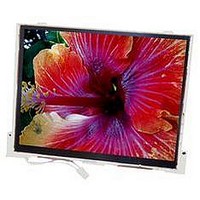
AND-TFT-8PA-KIT
Manufacturer Part Number
AND-TFT-8PA-KIT
Description
LCD Module Kit
Manufacturer
INTERFAN
Datasheet
1.AND-TFT-8PA-KIT.pdf
(7 pages)
Specifications of AND-TFT-8PA-KIT
Signal Input Type
NTSC, PAL
Rohs Compliant
Yes


Recommended Driving Conditions for Backlight
Interface Pin Assignment Connector:
Note 1: In order to satisfy the quality of B/L, no matter use what kind of inverter, the output lamp current must between Min. and Max. to avoid the abnormal dis-
play image caused by B/L. Note 2: The waveform of lamp driving voltage should be as closed to a perfect sine wave as possible.’ Note 3: The “Max of kick of
voltage” means the minimum voltage of inverter to turn on the CCFL and it should be applied to the lamp for more than 1 second to start up. Otherwise the lamp
may not be turned on.
1/28/08
Pin #.
10
11
12
13
14
15
16
17
18
19
20
21
22
23
24
25
26
27
28
29
30
31
32
1
2
3
4
5
6
7
8
9
Starting Voltage (25 °C)
Starting Voltage (0 °C)
(Reference Value)
(Reference Value)
Lamp Frequency
Lamp Voltage
Lamp Current
Symbol
Displays
VCOM
STH2
CPH3
CPH2
CPH1
VSS1
STH1
STVD
STVU
MOD
V
V
OEH
V
V
VCC
GND
Item
POL
VG+
VR+
OE1
OE2
OE3
CKV
VB+
V
Tel: 408.523.8200 • Fax: 408.733.1287 • sales@purdyelectronics.com • www.purdyelectronics.com
VB-
VG-
VR-
U/D
V
R/L
DD1
DD2
SS2
SS2
GH
EE
Purdy Electronics Corporation • 720 Palomar Avenue • Sunnyvale, CA 94085
I/O
I/O
I/O
I/O
I/O
–
–
–
–
–
–
–
–
–
I
I
I
I
I
I
I
I
I
I
I
I
I
I
I
I
I
I
I
Start pulse for source driver
Output enable for source driver
Polarity control for column inversion
Simultaneous/sequential mode select
Left/Right Control for source driver
Supply voltage of logic circuit for source driver
Sample and shift clock for source driver
Sample and shift clock for source driver
Sample and shift clock for source driver
Ground of logic circuit for source driver
Supply voltage of analog circuit for source driver
Video input B for negative polarity
Video input G for negative polarity
Video input R for negative polarity
Ground for analog circuit for source driver
Video input B for positive polarity
Video input G for positive polarity
Video input R for positive polarity
Ground for analog circuit for source driver
Start pulse for source driver
Voltage for common electrode
Output enable for gate driver
Output enable for gate driver
Output enable for gate driver
Up/Down Control for gate drive
Shift clock for gate driver
Vertical start pulse
Vertical start pulse
Power supply for gate driver circuit
Negative power gate driver
Positive power gate driver
Ground for gate driver
Symbol
V
V
V
P
I
L
S
S
L
L
Function
Remark
Note 2
Note 3
Note 3
Note1
Min.
540
30
4
–
–
Specifications
Remark
Typ.
Note 2
Note 2
Note 7
Note 6
Note 2
Note 1
Note 1
Note 1
Note 3
Note 4
Note 5
600
60
6
–
–
AND-TFT-8PA
Ta = 25°C
Max.
1100
660
920
80
8
Vrms
Vrms
Vrms
Unit
KHz
mA
4
Related parts for AND-TFT-8PA-KIT
Image
Part Number
Description
Manufacturer
Datasheet
Request
R

Part Number:
Description:
TFT COLOR TFT DISPLAY MODULES PROTOTYPE KITS
Manufacturer:
INTERFAN

Part Number:
Description:
LCD Module Kit
Manufacturer:
INTERFAN
Datasheet:

Part Number:
Description:
LCD Module Kit
Manufacturer:
INTERFAN
Datasheet:
Part Number:
Description:
LCD Module Kit
Manufacturer:
INTERFAN
Datasheet:

Part Number:
Description:
LCD Module Kit
Manufacturer:
INTERFAN
Datasheet:
Part Number:
Description:
TFT COLOR TFT DISPLAY MODULES PROTOTYPE KITS
Manufacturer:
INTERFAN
Part Number:
Description:
Seven-Segment Numeric LCD Display,3.5-CHARACTER,2-Edge
Manufacturer:
INTERFAN
Part Number:
Description:
Guard, Finger, Round, 2.81 Inch
Manufacturer:
INTERFAN
Datasheet:
Part Number:
Description:
FAN 25x10 5VDC 2.3CFM WIRE LEADS
Manufacturer:
AND OPTOELECTRONICS