HWK60000 Red Lion Controls, HWK60000 Datasheet - Page 2
HWK60000
Manufacturer Part Number
HWK60000
Description
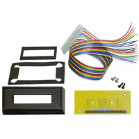
Bezel Kit, SCUBD
Manufacturer
Red Lion Controls
Datasheet
1.DM-OSC-B04A.pdf
(5 pages)
Specifications of HWK60000
Accessory Type
Bezel Kit
Lead Free Status / RoHS Status
Lead free / RoHS Compliant
For Use With/related Products
SubCub 2-8A, D, T
Lead Free Status / RoHS Status
Lead free / RoHS Compliant
Other names
HWK-60-000/A
HWK-60000
HWK6
RLC10
HWK-60000
HWK6
RLC10


DEVICE CONNECTIONS
TB12 - CMOS *Pulsed Pull-up Latched input. When input is connected to
TB11 - CMOS *Pulsed Pull-up Latched input. Adds 4 seconds to the total
TB10 - CMOS *Pulsed Pull-up Latched input. Adds 2 seconds to the total
TB9 - CMOS *Pulsed Pull-up Latched input. Adds 1 second to the total time
TB8 - CMOS *Pulsed Pull-up Latched input. Adds 1/2 second to the total
TB7 - CMOS *Pulsed Pull-up Latched input. Adds 1/4 second to the total
TB6 - CMOS *Pulsed Pull-up Latched input. Adds 1/8 second to the total
TB5 - CMOS *Pulsed Pull-up Latched input. Adds 1/16 second to the total
TB4 - CMOS *Pulsed Pull-up Latched input. Adds 1/32 second to the total
TB3 - CMOS *Pulsed Pull-up Latched input. Adds 1/64 second to the total
TB2 - CMOS *Pulsed Pull-up Latched input. Adds 1/128 second to the total
TB1 - CMOS *Pulsed Pull-up Latched input. Adds 1/256 second to the total
DPA - CMOS *Pulsed Pull-up Latched input. When used along with DPB,
DPB - CMOS *Pulsed Pull-up Latched input. When used along with DPA,
F.D. - CMOS *Pulsed Pull-up Latched input. When input is connected to V
M.R. - CMOS Internally Pulled-up input. When input is connected to V
* See section on “Pulsed Pull-Up Latched Inputs” for more information.
Note: For maximum noise immunity , connect all TB inputs to either V
CAUTION
handling to the same degree required by standard CMOS integrated circuits.
Units should be stored in the conductive packaging used to ship the devices.
Containers should be opened and units handled only on a conductive table
top by personnel wearing wrist-strap grounding equipment. These devices
have the same protection circuits as standard CMOS devices to prevent
damage to inputs due to nominal over-voltage.
V
connected to V
period.
time base period when input is connected to V
time base period when input is connected to V
base period when input is connected to V
time base period when input is connected to V
time base period when input is connected to V
time base period when input is connected to V
time base period when input is connected to V
time base period when input is connected to V
time base period when input is connected to V
time base period when input is connected to V
time base period when input is connected to V
selects the position of the decimal point.
selects the position of the decimal point.
Frequency Doubling is disabled. When input is connected to V
open, Frequency Doubling is enabled.
Master Reset will terminate the present time base period. When MR is
allowed to go high, the next time base period will begin. In normal use,
MR is connected to V
up Latched input.
V
noisey environments.
This device contains CMOS circuitry which requires special anti-static
SS
SS
, whichever is appropriate. Inputs left open may change states in some
, 8 seconds is added to the total time base period. When input is
ELECTRICAL CHARACTERISTICS V
SYMBOL
T
I
V
V
V
R
DDQ
V
I
I
V
I
ACC
DD
SIL
fc
SIH
DD
SIL
IH
PU
IH
IL
DD
or left open, no time is added to the total time base
DD
Input High Current (source)
or left open. Note that this is not a Pulsed Pull-
Time Base Accuracy
Pull Up Resistance
Input High Voltage
Input High Voltage
Input Low Voltage
Input Low Voltage
Signal Frequency
Supply Voltage
Supply Current
Supply Current
Input Leakage
PARAMETER
SS
.
SS
SS
SS
SS
SS
SS
SS
SS
SS.
SS.
.
.
.
.
.
.
.
.
0.05
MIN.
DD
2.5
3.9
50
= 5 V ±10% UNLESS OTHERWISE SPECIFIED
0.01
TYP.
DD
3.0
0.9
2.2
2.1
50
or left
DD
SS
SS
or
,
,
MAX.
200
500
6.0
0.5
0.1
55
45
2
SIG. - CMOS Schmidt trigger input. Counter chip increments on the falling
V
V
MAXIMUM RATINGS (VOLTAGE REF. TO V
RATING
DC Supply Voltage
Input Voltage, All Inputs
Operating Temperature*
Storage Temperature
* Extended high and low temperature ranges available, consult factory.
DD
SS
edge of the Signal input when F.D. is connected to V
chip increments on both rising and falling edges of the Signal input when
F.D. is connected to V
- Common for D.C. Supply and Inputs.
VDC
VDC
VDC
VDC
VDC
UNIT
- +2.5 to 6.0 VDC Supply
KW
µA
µA
µA
µA
%
TEST CONDITION
10 KHz signal, 1 second time base. All other inputs high.
1 second time base. All other inputs high.
Signal input only.
Signal input only.
All other inputs.
All other inputs.
V
All other inputs.
KHz
All pull-up inputs.
All time ranges.
DD
> V
IN
> V
DD
BLOCK DIAGRAM
SS
or left open (enabled).
SYMBOL
T
V
Signal input only.
T
V
STG
DD
A
I
-0.5 to (V
-0.5 to +6.5
-35 to +85
-35 to +85
VALUE
DD
SS
+0.5)
SS
(disabled). Counter
)
UNIT
VDC
VDC
o
o
C
C
Related parts for HWK60000
Image
Part Number
Description
Manufacturer
Datasheet
Request
R

Part Number:
Description:
Counter
Manufacturer:
Red Lion Controls
Datasheet:
Part Number:
Description:
Miniature Length Sensor
Manufacturer:
Red Lion Controls
Datasheet:
Part Number:
Description:
Model Lsc - Single Channel Output Length Sensor
Manufacturer:
Red Lion Controls
Datasheet: