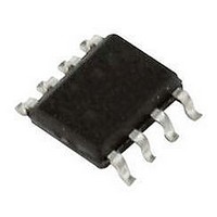
SMDA15C.TBT Semtech, SMDA15C.TBT Datasheet - Page 5

SMDA15C.TBT
Manufacturer Part Number
SMDA15C.TBT
Description
TVS DIODE ARRAY, 300W, 15V, SOIC
Manufacturer
Semtech
Specifications of SMDA15C.TBT
Reverse Stand-off Voltage Vrwm
15V
Breakdown Voltage Range
16.7V
Clamping Voltage Vc Max
30V
Diode Configuration
Bidirectional
Peak Pulse Current Ippm
10A
Diode Case Style
SOIC
No. Of Pins
8
Suppressor Type
TVS
Esd Protection Voltage
25KV@HBM
Direction Type
Bi-Directional
Configuration
Quad
Mounting Style
Surface Mount
Clamping Voltage (max)
30VV
Working Voltage (max)
15VV
Leakage Current (max)
1uAA
Capacitance Value
75pF
Operating Temperature Min Deg. C
-55C
Operating Temperature Max Deg. C
125C
Product Length (mm)
5mm
Product Depth (mm)
4mm
Product Height (mm)
1.5mm
Package / Case
SOIC
Pin Count
8
Rad Hardened
No
Lead Free Status / RoHS Status
Lead free / RoHS Compliant
Lead Free Status / RoHS Status
Lead free / RoHS Compliant
Available stocks
Company
Part Number
Manufacturer
Quantity
Price
Part Number:
SMDA15C.TBT
Manufacturer:
SEMTECH/美国升特
Quantity:
20 000
Device Connection for Protection of Five Data Lines
The SMDAxxC-5 is designed to protect up to 5 data or
I/O lines. They are bidirectional devices and may be
used on lines where the signal polarities are above and
below ground.
The SMDAxxC-5 TVS arrays employ a monolithic struc-
ture. Therefore, the working voltage (V
down voltage (V
tial voltage between any two data line pins. For ex-
ample, the SMDA24C-5 is designed for a maximum
voltage excursion of ±12V between any two data lines.
The device is connected as follows:
Circuit Board Layout Recommendations for Suppres-
sion of ESD.
Good circuit board layout is critical for the suppression
of ESD induced transients. The following guidelines are
recommended:
Matte Tin Lead Finish
Matte tin has become the industry standard lead-free
replacement for SnPb lead finishes. A matte tin finish
is composed of 100% tin solder with large grains.
Since the solder volume on the leads is small com-
pared to the solder paste volume that is placed on the
land pattern of the PCB, the reflow profile will be
determined by the requirements of the solder paste.
Therefore, these devices are compatible with both
PROTECTION PRODUCTS
PROTECTION PRODUCTS
Applications Information
2004 Semtech Corp.
Pins 1, 2, 3, 4, and 5 are connected to the lines
that are to be protected. Pin 8 is connected to
ground. The ground connections should be made
directly to the ground plane for best results. The
path length is kept as short as possible to reduce
the effects of parasitic inductance in the board
traces. Pins 6 and 7 are not connected.
Place the TVS near the input terminals or connec-
tors to restrict transient coupling.
Minimize the path length between the TVS and the
protected line.
Minimize all conductive loops including power and
ground loops.
The ESD transient return path to ground should be
kept as short as possible.
Never run critical signals near board edges.
Use ground planes whenever possible.
BR
) specifications apply to the differen-
RWM
) and break-
5
SMDA05C-5 THRU SMDA24C-5
lead-free and SnPb assembly techniques. In addition,
unlike other lead-free compositions, matte tin does not
have any added alloys that can cause degradation of
the solder joint.
DATA IN
DATA IN
Connection Diagram
Circuit Diagram
8
1
7
2
6
3
5
4
www.semtech.com
DATA OUT
DATA OUT


