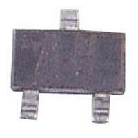
SLVU2.8.TCT Semtech, SLVU2.8.TCT Datasheet - Page 6

SLVU2.8.TCT
Manufacturer Part Number
SLVU2.8.TCT
Description
TVS DIODE, 400W, 2.8V, SOT-23
Manufacturer
Semtech
Datasheet
1.SLVU2.8.TCT.pdf
(10 pages)
Specifications of SLVU2.8.TCT
Diode Type
Unidirectional TVS
Clamping Voltage Vc Max
15V
Operating Voltage
2.8V
Diode Case Style
SOT-23
No. Of Pins
3
Peak Pulse Power Ppk @ 8x20us
400W
Junction Capacitance
10pF
Number Of Elements
1
Polarity
Uni-Directional
Package Type
SOT-23
Operating Temperature Classification
Military
Clamping Voltage
15V
Reverse Stand-off Voltage
2.8V
Leakage Current (max)
1uA
Peak Pulse Current
24A
Peak Pulse Power Dissipation
400W
Operating Temp Range
-55C to 125C
Mounting
Surface Mount
Pin Count
3
Breakdown Voltage Min
3V
Breakdown Voltage Vbr
40V
Capacitance, Cd
5pF
Rohs Compliant
Yes
Lead Free Status / RoHS Status
Lead free / RoHS Compliant
Lead Free Status / RoHS Status
Lead free / RoHS Compliant
Available stocks
Company
Part Number
Manufacturer
Quantity
Price
Company:
Part Number:
SLVU2.8.TCT
Manufacturer:
SEMTECH
Quantity:
3 549
Part Number:
SLVU2.8.TCT
Manufacturer:
SEMTECH/美国升特
Quantity:
20 000
not avalanche, but will “punch-through” to a conduct-
ing state. This structure results in a device with supe-
rior dc electrical parameters at low voltages while
maintaining the capability to absorb high transient
currents.
The IV characteristic curve of the EPD device is shown
in Figure 1. The device represents a high impedance
to the circuit up to the working voltage (V
transient event, the device will begin to conduct as it is
biased in the reverse direction. When the punch-
through voltage (V
low impedance state, diverting the transient current
away from the protected circuit. When the device is
conducting current, it will exhibit a slight “snap-back” or
negative resistance characteristic due to its structure.
This must be considered when connecting the device
to a power supply rail. To return to a non-conducting
state, the current through the device must fall below
the snap-back current (approximately < 50mA).
PROTECTION PRODUCTS
PROTECTION PRODUCTS
© 2008 Semtech Corp.
Applications Information (continued)
V
BRR
EPD TVS IV Characteristic Curve
PT
) is exceeded, the device enters a
I
I
I
I
SB
PT
PP
R
I
BRR
V
RWM
RWM
V
SB
). During a
V
PT
V
C
6
Circuit Board Layout Recommendations for Suppres-
sion of ESD.
Good circuit board layout is critical for the suppression
of ESD induced transients. The following guidelines are
recommended:
Matte Tin Lead Finish
Matte tin has become the industry standard lead-free
replacement for SnPb lead finishes. A matte tin finish
is composed of 100% tin solder with large grains.
Since the solder volume on the leads is small com-
pared to the solder paste volume that is placed on the
land pattern of the PCB, the reflow profile will be
determined by the requirements of the solder paste.
Therefore, these devices are compatible with both
lead-free and SnPb assembly techniques. In addition,
unlike other lead-free compositions, matte tin does not
have any added alloys that can cause degradation of
the solder joint.
Place the SLVU2.8 near the input terminals or
connectors to restrict transient coupling.
Minimize the path length between the TVS and the
protected line.
Minimize all conductive loops including power and
ground loops.
The ESD transient return path to ground should be
kept as short as possible.
Never run critical signals near board edges.
Use ground planes whenever possible.
Laser Diode Protection
SLVU2.8
www.semtech.com
SLVU2.8


