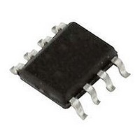
SRDA05-6.T Semtech, SRDA05-6.T Datasheet - Page 7

SRDA05-6.T
Manufacturer Part Number
SRDA05-6.T
Description
TVS DIODE ARRAY, 500W, 5V, SOIC
Manufacturer
Semtech
Datasheet
1.SRDA05-6.T.pdf
(9 pages)
Specifications of SRDA05-6.T
Diode Type
Low Capacitance
Clamping Voltage Vc Max
20V
Operating Voltage
1.5V
Diode Case Style
SOIC
No. Of Pins
8
Peak Pulse Power Ppk @ 8x20us
500W
Junction Capacitance
15pF
Breakdown Voltage Min
6V
Breakdown Voltage Vbr
6V
Capacitance, Cd
4pF
Rohs Compliant
Yes
Lead Free Status / RoHS Status
Lead free / RoHS Compliant
Available stocks
Company
Part Number
Manufacturer
Quantity
Price
Part Number:
SRDA05-6.TB
Manufacturer:
SEMTECH/美国升特
Quantity:
20 000
Company:
Part Number:
SRDA05-6.TBT
Manufacturer:
SEMTECH
Quantity:
367
Part Number:
SRDA05-6.TBT
Manufacturer:
SEMTECH/美国升特
Quantity:
20 000
Part Number:
SRDA05-6.TE
Manufacturer:
SEMTECH/美国升特
Quantity:
20 000
the current will be directed through the integrated TVS
diode to ground. The total clamping voltage seen by
the protected IC due to this path will be:
V
This is given in the data sheet as the rated clamping
voltage of the device. For an SRDA05-6 the typical
clamping voltage is <16V at I
internal to the RailClamp are low capacitance, fast
switching devices that are rated to handle high tran-
sient currents and maintain excellent forward voltage
characteristics.
Using the RailClamp does not negate the need for good
board layout. All other inductive paths must be consid-
ered. The connection between the positive supply and
the SRDA and from the ground plane to the SRDA
must be kept as short as possible. The path between
the SRDA and the protected line must also be mini-
mized. The protected lines should be routed directly to
the SRDA. Placement of the SRDA on the PC board is
also critical for effective ESD protection. The device
should be placed as close as possible to the input
connector. The reason for this is twofold. First,
inductance resists change in current flow. If a signifi-
cant inductance exists between the connector and the
TVS, the ESD current will be directed elsewhere (lower
resistance path) in the system. Second, the effects of
radiated emissions and transient coupling can cause
upset to other areas of the board even if there is no
direct path to the connector. By placing the TVS close
to the connector it will divert the ESD current immedi-
ately and absorb the ESD energy before it can be
coupled into nearby traces.
(Reference Semtech application note SI99-01 for
further information on board layout)
Matte Tin Lead Finish
Matte tin has become the industry standard lead-free
replacement for SnPb lead finishes. A matte tin finish
is composed of 100% tin solder with large grains.
Since the solder volume on the leads is small com-
pared to the solder paste volume that is placed on the
land pattern of the PCB, the reflow profile will be
PROTECTION PRODUCTS
PROTECTION PRODUCTS
© 2010 Semtech Corp.
Applications Information (continued)
C
= V
F(RailClamp)
+ V
TVS
PP
=30A. The diodes
7
determined by the requirements of the solder paste.
Therefore, these devices are compatible with both
lead-free and SnPb assembly techniques. In addition,
unlike other lead-free compositions, matte tin does not
have any added alloys that can cause degradation of
the solder joint.
SRDA3.3-6 and SRDA05-6
www.semtech.com


