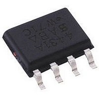
SLVU2.8-4.TET Semtech, SLVU2.8-4.TET Datasheet - Page 6

SLVU2.8-4.TET
Manufacturer Part Number
SLVU2.8-4.TET
Description
TVS DIODE ARRAY, 400W, 2.8V, SOIC
Manufacturer
Semtech
Datasheet
1.SLVU2.8-4.TBT.pdf
(9 pages)
Specifications of SLVU2.8-4.TET
Clamping Voltage Vc Max
15V
Operating Voltage
2.8V
Diode Case Style
SOIC
No. Of Pins
8
Peak Pulse Power Ppk @ 8x20us
400W
Peak Reflow Compatible (260 C)
Yes
Peak Pulse Current Ipp @ 8x20us
24A
Capacitance, Cd
5pF
No. Of Lines Protected Max
4
Rohs Compliant
Yes
Leaded Process Compatible
Yes
Package / Case
SO-8
Lead Free Status / RoHS Status
Lead free / RoHS Compliant
EPD TVS Characteristics
The SLVU2.8-4 is constructed using Semtech’s propri-
etary EPD technology. The structure of the EPD TVS is
vastly different from the traditional pn-junction devices.
At voltages below 5V, high leakage current and junction
capacitance render conventional avalanche technology
impractical for most applications. However, by utilizing
the EPD technology, the SLVU2.8-4 can effectively
operate at 2.8V while maintaining excellent electrical
characteristics.
The EPD TVS employs a complex nppn structure in
contrast to the pn structure normally found in tradi-
tional silicon-avalanche TVS diodes. The EPD mecha-
nism is achieved by engineering the center region of
the device such that the reverse biased junction does
not avalanche, but will “punch-through” to a conduct-
ing state. This structure results in a device with supe-
rior dc electrical parameters at low voltages while
maintaining the capability to absorb high transient
currents.
The IV characteristic curve of the EPD device is shown
in Figure 1. The device represents a high impedance
to the circuit up to the working voltage (V
transient event, the device will begin to conduct as it is
biased in the reverse direction. When the punch-
through voltage (V
low impedance state, diverting the transient current
away from the protected circuit. When the device is
conducting current, it will exhibit a slight “snap-back” or
negative resistance characteristic due to its structure.
This must be considered when connecting the device
to a power supply rail. To return to a non-conducting
state, the current through the device must fall below
the snap-back current (approximately < 50mA).
PROTECTION PRODUCTS
Applications Information (continued)
2008 Semtech Corp.
PT
) is exceeded, the device enters a
RWM
). During a
6
V
BRR
EPD TVS IV Characteristic Curve
I
I
I
I
SB
PT
PP
R
I
BRR
SLVU2.8-4
V
RWM
www.semtech.com
V
SB
V
PT
V
C


