2N5911 Vishay, 2N5911 Datasheet

MATCHED N CH JFET PAIR, -25V, TO-78

2N5911

Manufacturer Part Number
2N5911
Description
MATCHED N CH JFET PAIR, -25V, TO-78
Manufacturer
Vishay
Datasheets

Specifications of 2N5911

Breakdown Voltage Vbr
-25V
Gate-source Cutoff Voltage Vgs(off) Max
-5V
Power Dissipation Pd
500mW
Operating Temperature Range
-55°C To +150°C
No. Of Pins
6
Continuous Drain Current Id
40mA
Channel Type
N
Configuration
Dual
Gate-source Voltage (max)
25V
Drain-gate Voltage (max)
-25V
Operating Temperature (min)
-55C
Operating Temperature (max)
150C
Operating Temperature Classification
Military
Mounting
Through Hole
Pin Count
7
Package Type
TO-78
Lead Free Status / RoHS Status
Contains lead / RoHS non-compliant
The 2N5911/5912 are matched pairs of JFETs mounted in a
TO-78 package. This two-chip design reduces parasitics and
gives better performance at high frequencies while ensuring
extremely tight matching.
The hermetically-sealed TO-78 package is available with full
military screening per MIL-S-19500 (see Military Information).
Gate-Drain, Gate-Source Voltage
Gate-Gate Voltage
Gate Current
Lead Temperature (
Storage Temperature
Operating Junction Temperature
For applications information see AN102.
Document Number: 70255
S-04031—Rev. D, 04-Jun-01
D Two-Chip Design
D High Slew Rate
D Low Offset/Drift Voltage
D Low Gate Leakage: 1 pA
D Low Noise
D High CMRR: 85 dB
Part Number
2N5911
2N5912
. . . . . . . . . . . . . . . . . . . . . . . . . . . . . . . . . . . . . . . . . . . . . . . . .
. . . . . . . . . . . . . . . . . . . . . . . . . . . . . . . . . . . . . . . . . . . .
1
/
16
. . . . . . . . . . . . . . . . . . . . . . . . . . . . . . . . . . .
V
” from case for 10 sec.)
GS(off)
–1 to –5
–1 to –5
. . . . . . . . . . . . . . . . . . . . . . . . . .
(V)
. . . . . . . . . . . . . . . . . . . . . . . . . . . . . . .
V
D Minimum Parasitics Ensuring Maximum
D Improved Op Amp Speed, Settling Time Accuracy
D Minimum Input Error/Trimming Requirement
D Insignificant Signal Loss/Error Voltage
D High System Sensitivity
D Minimum Error with Large Input Signal
(BR)GSS
Matched N-Channel JFET Pairs
High-Frequency Performance
. . . . . . . . . . . . . . . . . . .
–25
–25
Min (V)
D
1
–65 to 200_C
–55 to 150_C
G
S
1
1
2
g
fs
"80 V
50 mA
300_C
–25 V
1
3
Min (mS)
5
5
Top View
TO-78
Case
4
For
SST440/SST441, the TO-71 packaged U440/U441, the
low-noise SST/U401 series, and the low-leakage U421/423
data sheets.
Power Dissipation :
Notes
a.
b.
I
G
5
7
Derate 3 mW/_C above 25_C
Derate 4 mW/_C above 25_C
Typ (pA)
6
G
–1
–1
similar
S
2
2
D
2
jV
products
GS1
– V
D Wideband Differential Amps
D High-Speed, Temp-Compensated,
D High Speed Comparators
D Impedance Converters
Per Side
Total
Single-Ended Input Amps
GS2
b
10
15
. . . . . . . . . . . . . . . . . . . . . . . . . . .
see
j Max (mV)
a
. . . . . . . . . . . . . . . . . . . . . . . .
Vishay Siliconix
the
2N5911/5912
SO-8
www.vishay.com
packaged
367 mW
500 mW
8-1

Related parts for 2N5911

2N5911 Summary of contents

Page 1

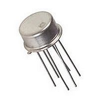
... D Low Noise D High System Sensitivity D High CMRR Minimum Error with Large Input Signal The 2N5911/5912 are matched pairs of JFETs mounted in a TO-78 package. This two-chip design reduces parasitics and gives better performance at high frequencies while ensuring extremely tight matching. The hermetically-sealed TO-78 package is available with full military screening per MIL-S-19500 (see Military Information) ...

Page 2

... DG D GS2 | GS2 T = –55 to 125_C kHz | mA 125_C Limits 2N5911 2N5912 a Typ Min Max Min Max –35 –25 –25 –3.5 –1 –5 –1 – –1 –100 –100 –2 –250 –250 –1 –100 –100 –0.3 –100 –100 –1.5 –0.3 –4 –0.3 –4 0.7 ...

Page 3

... S-04031—Rev. D, 04-Jun- 100 100 0.1 pA –6 –8 – –0.2 V –0.4 V –0.6 V –0.8 V –1.0 V –1 –0.2 V –0.4 V –0.6 V –0.8 V –1.0 V –1.2 V 0.8 1 2N5911/5912 Vishay Siliconix Gate Leakage Current G(on 125_C 125_C GSS 25_C GSS – Drain-Gate Voltage (V) DG Output Characteristics –5 V GS(off ...

Page 4

... Vishay Siliconix Transfer Characteristics –2 V GS(off –55_C A 6 25_C 4 125_C –0.4 –0.8 –1.2 V – Gate-Source Voltage (V) GS Transconductance vs. Gate-Source Voltage –2 V GS(off –55_C A 25_C 6 125_C –0.4 –0.8 –1.2 V – Gate-Source Voltage (V) GS Circuit Voltage Gain vs. Drain Current –2 V GS(off Assume V ...

Page 5

... Frequency (MHz) Document Number: 70255 S-04031—Rev. D, 04-Jun- –16 –20 100 10 0.1 1000 500 100 10 0.1 500 1000 2N5911/5912 Vishay Siliconix Common-Source Reverse Feedback Capacitance vs. Gate-Source Voltage MHz –4 –8 –12 –16 V – Gate-Source Voltage (V) GS ...

Page 6

... Vishay Siliconix Equivalent Input Noise Voltage vs. Frequency 100 – Frequency (Hz) On-Resistance and Output Conductance vs. Gate-Source Cutoff Voltage 200 160 120 mA kHz 0 0 –2 –4 V – Gate-Source Cutoff Voltage (V) GS(off) www.vishay.com 8 100 k 200 g os 160 120 –6 –8 –10 Output Conductance vs. Drain Current ...

Page 7

... Vishay disclaims any and all liability arising out of the use or application of any product described herein or of any information provided herein to the maximum extent permitted by law. The product specifications do not expand or otherwise modify Vishay’ ...

Related keywords