IRF740PBF Vishay, IRF740PBF Datasheet - Page 6
IRF740PBF
Manufacturer Part Number
IRF740PBF
Description
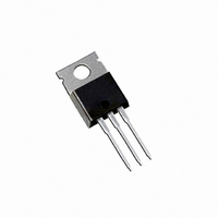
N CHANNEL MOSFET, 400V, 10A, TO-220
Manufacturer
Vishay
Specifications of IRF740PBF
Transistor Polarity
N Channel
Continuous Drain Current Id
10A
Drain Source Voltage Vds
400V
On Resistance Rds(on)
550mohm
Rds(on) Test Voltage Vgs
10V
Threshold Voltage Vgs Typ
4V
Fet Type
MOSFET N-Channel, Metal Oxide
Fet Feature
Standard
Rds On (max) @ Id, Vgs
550 mOhm @ 6A, 10V
Drain To Source Voltage (vdss)
400V
Current - Continuous Drain (id) @ 25° C
10A
Vgs(th) (max) @ Id
4V @ 250µA
Gate Charge (qg) @ Vgs
63nC @ 10V
Input Capacitance (ciss) @ Vds
1400pF @ 25V
Power - Max
125W
Mounting Type
Through Hole
Package / Case
TO-220-3 (Straight Leads)
Minimum Operating Temperature
- 55 C
Configuration
Single
Resistance Drain-source Rds (on)
0.55 Ohm @ 10 V
Drain-source Breakdown Voltage
400 V
Gate-source Breakdown Voltage
+/- 20 V
Continuous Drain Current
10 A
Power Dissipation
125000 mW
Maximum Operating Temperature
+ 150 C
Mounting Style
Through Hole
Lead Free Status / RoHS Status
Lead free / RoHS Compliant
Lead Free Status / RoHS Status
Lead free / RoHS Compliant, Lead free / RoHS Compliant
Other names
*IRF740PBF
Available stocks
Company
Part Number
Manufacturer
Quantity
Price
Company:

Part Number:
IRF740PBF
Manufacturer:
MITSUBISHI
Quantity:
56
Company:
Part Number:
IRF740PBF
Manufacturer:
VISHAY
Quantity:
200
Part Number:
IRF740PBF
Manufacturer:
IR
Quantity:
20 000


IRF740, SiHF740
Vishay Siliconix
www.vishay.com
6
THE PRODUCT DESCRIBED HEREIN AND THIS DATASHEET ARE SUBJECT TO SPECIFIC DISCLAIMERS, SET FORTH AT
Vary t
required I
Fig. 12a - Unclamped Inductive Test Circuit
10 V
p
Fig. 13a - Basic Gate Charge Waveform
to obtain
V
G
AS
R
10 V
Q
G
GS
V
DS
t
p
Charge
Q
Q
GD
G
I
AS
D.U.T
0.01 Ω
L
Fig. 12c - Maximum Avalanche Energy vs. Drain Current
91054_12c
1000
This datasheet is subject to change without notice.
1200
600
800
400
200
0
25
V
DD
+
-
= 50 V
Starting T
V
DD
50
J
, Junction Temperature (°C)
75
100
Top
Bottom
Fig. 12b - Unclamped Inductive Waveforms
V
125
I
AS
DS
12 V
Fig. 13b - Gate Charge Test Circuit
V
GS
4.5 A
5.3 A
Same type as D.U.T.
10 A
I
Current regulator
D
150
0.2 µF
Current sampling resistors
3 mA
50 kΩ
t
0.3 µF
p
I
G
S11-0507-Rev. C, 21-Mar-11
www.vishay.com/doc?91000
Document Number: 91054
D.U.T.
V
I
DS
D
+
V
-
V
DD
DS
Related parts for IRF740PBF
Image
Part Number
Description
Manufacturer
Datasheet
Request
R


Part Number:
Description:
357-036-542-201 CARDEDGE 36POS DL .156 BLK LOPRO
Manufacturer:
Vishay
Datasheet:
Part Number:
Description:
357-036-542-201 CARDEDGE 36POS DL .156 BLK LOPRO
Manufacturer:
Vishay
Datasheet:
Part Number:
Description:
357-036-542-201 CARDEDGE 36POS DL .156 BLK LOPRO
Manufacturer:
Vishay
Datasheet:
Part Number:
Description:
357-036-542-201 CARDEDGE 36POS DL .156 BLK LOPRO
Manufacturer:
Vishay
Datasheet:
Part Number:
Description:
357-036-542-201 CARDEDGE 36POS DL .156 BLK LOPRO
Manufacturer:
Vishay
Datasheet:
Part Number:
Description:
357-036-542-201 CARDEDGE 36POS DL .156 BLK LOPRO
Manufacturer:
Vishay
Datasheet:
Part Number:
Description:
357-036-542-201 CARDEDGE 36POS DL .156 BLK LOPRO
Manufacturer:
Vishay
Datasheet:
Part Number:
Description:
357-036-542-201 CARDEDGE 36POS DL .156 BLK LOPRO
Manufacturer:
Vishay
Datasheet:
Part Number:
Description:
357-036-542-201 CARDEDGE 36POS DL .156 BLK LOPRO
Manufacturer:
Vishay
Datasheet:
Part Number:
Description:
357-036-542-201 CARDEDGE 36POS DL .156 BLK LOPRO
Manufacturer:
Vishay
Datasheet:
Part Number:
Description:
357-036-542-201 CARDEDGE 36POS DL .156 BLK LOPRO
Manufacturer:
Vishay
Datasheet:
Part Number:
Description:
357-036-542-201 CARDEDGE 36POS DL .156 BLK LOPRO
Manufacturer:
Vishay
Datasheet:
Part Number:
Description:
357-036-542-201 CARDEDGE 36POS DL .156 BLK LOPRO
Manufacturer:
Vishay
Datasheet:
Part Number:
Description:
357-036-542-201 CARDEDGE 36POS DL .156 BLK LOPRO
Manufacturer:
Vishay
Datasheet: