2N3055H MULTICOMP, 2N3055H Datasheet - Page 2
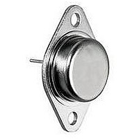
2N3055H
Manufacturer Part Number
2N3055H
Description
BIPOLAR TRANSISTOR, NPN, 60V
Manufacturer
MULTICOMP
Datasheet
1.2N3055H.pdf
(4 pages)
Specifications of 2N3055H
Transistor Polarity
NPN
Collector Emitter Voltage V(br)ceo
60V
Transition Frequency Typ Ft
800kHz
Power Dissipation Pd
115W
Dc Collector Current
15A
Dc Current Gain Hfe
20
Lead Free Status / RoHS Status
Lead free / RoHS Compliant


Î Î Î Î Î Î Î Î Î Î Î Î Î Î Î Î Î Î Î Î Î Î
Î Î Î Î Î Î Î Î Î Î Î Î Î Î Î Î Î Î Î Î Î Î
Î Î Î Î Î Î Î Î Î Î Î Î Î Î Î Î Î Î Î Î Î Î
Î Î Î Î Î Î Î Î Î Î Î Î Î Î Î Î Î Î Î Î Î Î
Î Î Î Î Î Î Î Î Î Î Î Î Î Î Î Î Î Î Î Î Î Î
Î Î Î Î Î Î Î Î Î Î Î Î Î Î Î Î Î Î Î Î Î Î
Î Î Î Î Î Î Î Î Î Î Î Î Î Î Î Î Î Î Î Î Î Î
Î Î Î Î Î Î Î Î Î Î Î Î Î Î Î Î Î Î Î Î Î Î
Î Î Î Î Î Î Î Î Î Î Î Î Î Î Î Î Î Î Î Î Î Î
Î Î Î Î Î Î Î Î Î Î Î Î Î Î Î Î Î Î Î Î Î Î
Î Î Î Î Î Î Î Î Î Î Î Î Î Î Î Î Î Î Î Î Î Î
Î Î Î Î Î Î Î Î Î Î Î Î Î Î Î Î Î Î Î Î Î Î
Î Î Î Î Î Î Î Î Î Î Î Î Î Î Î Î Î Î Î Î Î Î
Î Î Î Î Î Î Î Î Î Î Î Î Î Î Î Î Î Î Î Î Î Î
Î Î Î Î Î Î Î Î Î Î Î Î Î Î Î Î Î Î Î Î Î Î
Î Î Î Î Î Î Î Î Î Î Î Î Î Î Î Î Î Î Î Î Î Î Î Î Î Î Î Î Î Î Î Î Î
Î Î Î Î Î Î Î Î Î Î Î Î Î Î Î Î Î Î Î Î Î Î Î Î Î Î Î Î Î Î Î Î Î
Î Î Î Î Î Î Î Î Î Î Î Î Î Î Î Î Î Î Î Î Î Î Î Î Î Î Î Î Î Î Î Î Î
Î Î Î Î Î Î Î Î Î Î Î Î Î Î Î Î Î Î Î Î Î Î Î Î Î Î Î Î Î Î Î Î Î
Î Î Î Î Î Î Î Î Î Î Î Î Î Î Î Î Î Î Î Î Î Î
Î Î Î Î Î Î Î Î Î Î Î Î Î Î Î Î Î Î Î Î Î Î
Î Î Î Î Î Î Î Î Î Î Î Î Î Î Î Î Î Î Î Î Î Î Î Î Î Î Î Î Î Î Î Î Î
Î Î Î Î Î Î Î Î Î Î Î Î Î Î Î Î Î Î Î Î Î Î Î Î Î Î Î Î Î Î Î Î Î
Î Î Î Î Î Î Î Î Î Î Î Î Î Î Î Î Î Î Î Î Î Î
Î Î Î Î Î Î Î Î Î Î Î Î Î Î Î Î Î Î Î Î Î Î
Î Î Î Î Î Î Î Î Î Î Î Î Î Î Î Î Î Î Î Î Î Î
Î Î Î Î Î Î Î Î Î Î Î Î Î Î Î Î Î Î Î Î Î Î
Î Î Î Î Î Î Î Î Î Î Î Î Î Î Î Î Î Î Î Î Î Î
Î Î Î Î Î Î Î Î Î Î Î Î Î Î Î Î Î Î Î Î Î Î
*OFF CHARACTERISTICS
*ON CHARACTERISTICS (Note 1)
SECOND BREAKDOWN
DYNAMIC CHARACTERISTICS
ELECTRICAL CHARACTERISTICS
Collector−Emitter Sustaining Voltage (Note 1)
(I
Collector−Emitter Sustaining Voltage (Note 1)
(I
Collector Cutoff Current
(V
Collector Cutoff Current
(V
(V
Emitter Cutoff Current
(V
DC Current Gain
(I
(I
Collector−Emitter Saturation Voltage
(I
(I
Base−Emitter On Voltage
(I
Second Breakdown Collector Current with Base Forward Biased
(V
Current Gain − Bandwidth Product
(I
*Small−Signal Current Gain
(I
*Small−Signal Current Gain Cutoff Frequency
(V
*Indicates Within JEDEC Registration. (2N3055)
1. Pulse Test: Pulse Width v 300 ms, Duty Cycle v 2.0%.
C
C
C
C
C
C
C
C
C
CE
CE
CE
BE
CE
CE
0.6
0.4
0.2
20
10
= 200 mAdc, I
= 200 mAdc, R
= 4.0 Adc, V
= 10 Adc, V
= 4.0 Adc, I
= 10 Adc, I
= 4.0 Adc, V
= 0.5 Adc, V
= 1.0 Adc, V
6
4
2
1
Figure 2. Active Region Safe Operating Area
= 7.0 Vdc, I
= 30 Vdc, I
= 100 Vdc, V
= 100 Vdc, V
= 40 Vdc, t = 1.0 s, Nonrepetitive)
= 4.0 Vdc, I
6
V
CE
B
, COLLECTOR−EMITTER VOLTAGE (VOLTS)
B
CE
CE
CE
CE
CE
= 3.3 Adc)
BONDING WIRE LIMIT
THERMALLY LIMITED @ T
SECOND BREAKDOWN LIMIT
B
= 400 mAdc)
C
C
B
10
= 0)
= 4.0 Vdc)
BE
BE(off)
BE(off)
= 0)
= 4.0 Vdc)
= 4.0 Vdc)
= 10 Vdc, f = 1.0 MHz)
= 4.0 Vdc, f = 1.0 kHz)
= 1.0 Adc, f = 1.0 kHz)
= 0)
= 100 W)
= 1.5 Vdc)
= 1.5 Vdc, T
dc
500 ms
20
Characteristic
C
1 ms
= 150 C)
C
= 25 C (SINGLE PULSE)
(T
C
250 ms
= 25 C unless otherwise noted)
40
2N3055, MJ2955
http://onsemi.com
50 ms
60
2
a transistor: average junction temperature and second
breakdown. Safe operating area curves indicate I
limits of the transistor that must be observed for reliable
operation; i.e., the transistor must not be subjected to greater
dissipation than the curves indicate.
variable depending on power level. Second breakdown
pulse limits are valid for duty cycles to 10% but must be
derated for temperature according to Figure 1.
There are two limitations on the power handling ability of
The data of Figure 2 is based on T
Î Î Î Î Î
Î Î Î Î Î
Î Î Î Î Î
Î Î Î Î Î
Î Î Î Î Î
Î Î Î Î Î
Î Î Î Î Î
Î Î Î Î Î
Î Î Î Î Î
Î Î Î Î Î
Î Î Î Î Î
Î Î Î Î Î
Î Î Î Î Î
Î Î Î Î Î
Î Î Î Î Î
Î Î Î Î Î
Î Î Î Î Î
Î Î Î Î Î
Î Î Î Î Î
Î Î Î Î Î
Î Î Î Î Î
Î Î Î Î Î
Î Î Î Î Î
V
V
Symbol
V
V
CEO(sus)
CER(sus)
I
CE(sat)
I
I
BE(on)
h
CEO
EBO
CEX
I
f
h
hfe
s/b
f
FE
T
fe
Î Î Î
Î Î Î
Î Î Î
Î Î Î
Î Î Î
Î Î Î
Î Î Î
Î Î Î
Î Î Î
Î Î Î
Î Î Î
Î Î Î
Î Î Î
Î Î Î
Î Î Î
Î Î Î
Î Î Î
Î Î Î
Î Î Î
Î Î Î
Î Î Î
Î Î Î
Î Î Î
2.87
Min
5.0
2.5
60
70
20
15
10
−
−
−
−
−
−
Î Î Î Î
Î Î Î Î
Î Î Î Î
Î Î Î Î
Î Î Î Î
Î Î Î Î
Î Î Î Î
Î Î Î Î
Î Î Î Î
Î Î Î Î
Î Î Î Î
Î Î Î Î
Î Î Î Î
Î Î Î Î
Î Î Î Î
Î Î Î Î
Î Î Î Î
Î Î Î Î
Î Î Î Î
Î Î Î Î
Î Î Î Î
Î Î Î Î
Î Î Î Î
C
= 25 C; T
Max
120
0.7
1.0
5.0
5.0
1.1
3.0
1.5
70
−
−
−
−
−
−
Î Î Î
Î Î Î
Î Î Î
Î Î Î
Î Î Î
Î Î Î
Î Î Î
Î Î Î
Î Î Î
Î Î Î
Î Î Î
Î Î Î
Î Î Î
Î Î Î
Î Î Î
Î Î Î
Î Î Î
Î Î Î
Î Î Î
Î Î Î
Î Î Î
Î Î Î
Î Î Î
C
mAdc
mAdc
mAdc
MHz
Unit
Vdc
Vdc
Vdc
Vdc
Adc
kHz
J(pk)
− V
−
−
CE
is
Related parts for 2N3055H
Image
Part Number
Description
Manufacturer
Datasheet
Request
R

Part Number:
Description:
IC, LINEAR VOLTAGE REGULATOR, 15V, TO-92
Manufacturer:
MULTICOMP
Datasheet:

Part Number:
Description:
Switch Cap
Manufacturer:
MULTICOMP
Datasheet:

Part Number:
Description:
COAXIAL CABLE, 100MM, BLACK
Manufacturer:
MULTICOMP
Datasheet:

Part Number:
Description:
FUSE, PTC RESET, 16V, 3A, RADIAL
Manufacturer:
MULTICOMP
Datasheet:
Part Number:
Description:
FUSE, PTC RESET, 16V, 5A, RADIAL
Manufacturer:
MULTICOMP
Datasheet:

Part Number:
Description:
FUSE, PTC RESET, 30V, 1.85A, RADIAL
Manufacturer:
MULTICOMP
Datasheet:

Part Number:
Description:
FUSE, PTC RESET, 30V, 4A, RADIAL
Manufacturer:
MULTICOMP
Datasheet:

Part Number:
Description:
FUSE, PTC RESET, 60V, 170mA, RADIAL
Manufacturer:
MULTICOMP
Datasheet:

Part Number:
Description:
FUSE, PTC RESET, 90V, 200mA, RADIAL
Manufacturer:
MULTICOMP
Datasheet:
Part Number:
Description:
FUSE, PTC RESET, 90V, 250mA, RADIAL
Manufacturer:
MULTICOMP
Datasheet:
Part Number:
Description:
FUSE, PTC RESET, 90V, 400mA, RADIAL
Manufacturer:
MULTICOMP
Datasheet:
Part Number:
Description:
FUSE, PTC RESET, 90V, 900mA, RADIAL
Manufacturer:
MULTICOMP
Datasheet:

Part Number:
Description:
FUSE, PTC RESET, 90V, 1.6A, RADIAL
Manufacturer:
MULTICOMP
Datasheet:
Part Number:
Description:
FUSE, PTC RESET, 90V, 1.85A, RADIAL
Manufacturer:
MULTICOMP
Datasheet:

Part Number:
Description:
FUSE, PTC RESET, 16V, 750mA, SMD
Manufacturer:
MULTICOMP
Datasheet: