TC65 TERMINAL SIEMENS, TC65 TERMINAL Datasheet - Page 35
TC65 TERMINAL
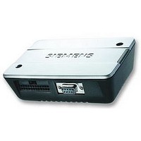
Manufacturer Part Number
TC65 TERMINAL
Description
GSM/GPRS JAVA TERMINAL PACK
Manufacturer
SIEMENS
Datasheet
1.TC65_TERMINAL.pdf
(58 pages)
Specifications of TC65 TERMINAL
Rohs Compliant
YES


GPIO-
Connector
3.10.5
The two balanced analog inputs are used for measuring external DC voltages in a range of 0V to
5.0V.
Note: Only positive differential voltage can be handled because of the input requirement of ADC.
Table 10: ADC signal description
Use the command AT^SRADC described in [1] to configure the analog inputs and to get the
measurement results.
Note:
It is necessary to recalculate measurement results because an amplifier is used to scale down the
ADCx_IN input voltage of the TC65 Terminal (5V) to the ADCx_IN input voltage of the in-built TC65
module (2.4V).
Two parameters (determined and stored by factory) have to be used for offset compensation and for
consideration of gain and tolerances:
Use the command AT^SAADC described in [1] to read out the required parameters:
<ofsx>: Offset
<ampx> : Amplification factor (Gain*4096)
To recalculate the exact voltages [mV] measured at the ADCx_IN input use the following equation:
Value[mV] = (<value> from AT^SRADC - <ofsx>) * <ampx> / 4096
TC65 Terminal_HD_V01.041
TC65 Terminal Hardware Interface Description
Strictly Confidential / Released
Signal name
ADC1_IN_N
ADC1_IN_P
ADC2_IN_N
ADC2_IN_P
ADCx_IN_N
ADCx_IN_P
Analog-to Digital Converter (ADC)
21,9
22,10
22
21
10
9
Pin
6V transil diods
for ESD protection
0V...5.0V
Description
Negative voltage
Positive voltage (must be more positive than ADC2_IN_N)
Negative voltage
Positive voltage (must be more positive than ADC2_IN_N)
Figure 12: ADC balanced amplifier
475k
475k
Gain = appr. 0.48
Page 35 of 58
x=1 for Input 1 or 2 for input 2
2x150k
G=2
0V...2.4V
2,3
56
s
ADCx_IN
AGND
29.09.2005
Cellular
Engine
TC65
Related parts for TC65 TERMINAL
Image
Part Number
Description
Manufacturer
Datasheet
Request
R

Part Number:
Description:
CAP ALUM 20UF 350V AXIAL
Manufacturer:
Cornell Dubilier Electronics (CDE)
Datasheet:

Part Number:
Description:
Intel 80C32 - Siemens SAB-C501, Nearest Equivalent Replacement
Manufacturer:
Siemens Semiconductor Group
Part Number:
Description:
IGBT MODULE
Manufacturer:
Siemens Semiconductor Group
Datasheet:
Part Number:
Description:
SIMOPAC Module (Power module Single switch N channel Enhancement mode)
Manufacturer:
Siemens Semiconductor Group
Datasheet:
Part Number:
Description:
(BSMxxx) TRANSISTOR
Manufacturer:
Siemens Semiconductor Group
Datasheet:
Part Number:
Description:
SIMOPAC Module (Power module Single switch N channel Enhancement mode)
Manufacturer:
Siemens Semiconductor Group
Datasheet:
Part Number:
Description:
main ratings
Manufacturer:
Siemens Semiconductor Group
Datasheet:
Part Number:
Description:
Manufacturer:
Siemens Semiconductor Group
Datasheet:
Part Number:
Description:
Manufacturer:
Siemens Semiconductor Group
Datasheet:
Part Number:
Description:
Manufacturer:
Siemens Semiconductor Group
Datasheet:
Part Number:
Description:
ICs for Consumer Electronics
Manufacturer:
Siemens Semiconductor Group
Datasheet:
Part Number:
Description:
Video and Sound IF with V & S SCART
Manufacturer:
Siemens Semiconductor Group
Datasheet:
Part Number:
Description:
Manufacturer:
Siemens Semiconductor Group
Datasheet:
Part Number:
Description:
Multistandard Sound IF
Manufacturer:
Siemens Semiconductor Group
Datasheet: