DD-160128FC-1A DENSITRON, DD-160128FC-1A Datasheet
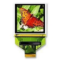
DD-160128FC-1A
Specifications of DD-160128FC-1A


Related parts for DD-160128FC-1A


DD-160128FC-1A Summary of contents
Page 1
... ‐ Frame rate : 90 frames/sec( 75.0 ~ 150.0 frames/sec adjustable) ▪ Supply Voltage ‐ VDD : 2.4 ~ 3.3V ‐ VDDH : 8.0 ~ 18.0V ‐ VDDIO : 1.6 ~ 3.3V ...
Page 2
SYNCOAM Co., Ltd. SEPS525 ...
Page 3
... MPU For an 68‐system bus interface, bus enable strobe(active high) When using SPI, fix it to VDD or VSS level For an 80‐system bus interface, write strobe signal(active low) For an 68‐system bus interface, read/write select ...
Page 4
... Data written into the DDRAM from the MPU is first written into the WDR and then it is automatically ...
Page 5
... SYNCOAM Co., Ltd. SEPS525 Version: 0.2 1) 18‐bit Bus Interface (Index 16h) DFM1 DFM0 0 0 Index/Command Write DDRAM Read/Write TRI Operation x 18‐bit bus operation 5/45 ...
Page 6
... SYNCOAM Co., Ltd. SEPS525 Version: 0.2 2) 16‐bit Bus Interface DFM1 DFM0 0 1 Index/Command Write DDRAM Read/Write ...
Page 7
... SYNCOAM Co., Ltd. SEPS525 Version: 0.2 3) 9‐bit Bus Interface DFM1 DFM0 1 0 Index/Command Write DDRAM Read/Write ...
Page 8
... DFM1 DFM0 1 0 1 1 Index/Command Write DDRAM Write/Read DDRAM Write/Read (TRI mode) TRI Operation 0 Dual 8‐bit 1 Triple 6‐bit ...
Page 9
SYNCOAM Co., Ltd. SEPS525 ...
Page 10
SYNCOAM Co., Ltd. SEPS525 ...
Page 11
... The 18‐bit RGB interface is selected by setting RIM[1:0] bits to “00”. DDRAM write operation is Synchronized with DOTCLK and ENABLE. Display data are transmitted to DDRAM in synchronization ...
Page 12
... The 16‐bit RGB interface is selected by setting RIM[1:0] bits to “01”. DDRAM write operation is Synchronized with DOTCLK and ENABLE. Display data are transmitted to DDRAM in synchronization ...
Page 13
... The 6‐bit RGB interface is selected by setting RIM[1:0] bits to “10”. DDRAM write operation is Synchronized with DOTCLK and ENABLE. Display data are transmitted to DDRAM in synchronization with 6‐bit RGB ...
Page 14
... The DDRAM stores pixel data for the display. It is composed of 128‐row by 160‐column x 18‐bit addressable array. Address counter provides row and column address to DDRAM for access display pixel data from ...
Page 15
... When data is written to the on‐chip DDRAM, a window address‐range which is specified by the horizontal address register(start : MX1[7:0], end : MX2[7:0]) or the vertical address register(start : MY1[7:0], end : ...
Page 16
... 10. Display ON/OFF : OFF 11. Panel display size : FX1 = 00h, FX2 = 9Fh, FY1 = 00h, FY2 = 7Fh 12. Display data RAM read column/row address : FAC = 00h, FAR = 00h 13. Precharge time(R/G/B) : 0 clock ...
Page 17
... DGAMMA0 GRAY_SCALE _TABLE_DATA DUTY1 DUTY0 DUTY DSL1 DSL0 DSL FAC1 FAC0 D1_DDRAM_FAC FAR1 FAR0 D1_DDRAM_FAR SAC1 SAC0 D2_DDRAM_SAC SAR1 SAR0 D2_DDRAM_SAR ...
Page 18
... HC : Horizontal address increment/decrement at memory write mode. VC : Vertical address increment/decrement at memory write mode. HV : Automatic update method of the AC(means internal address counter). HV=0(horizontal), HV=1(vertical) SWAP : Swap between R and B. ...
Page 19
SYNCOAM Co., Ltd. SEPS525 ...
Page 20
... RC : Reduced driving current. When RC = 0, Normal When RC = 1, 1/2driving current(address 0x10, 0x11, 0x12) OSCPS : Oscillator power down When OSCPS = 0, Normal ...
Page 21
SYNCOAM Co., Ltd. SEPS525 ...
Page 22
SYNCOAM Co., Ltd. SEPS525 ...
Page 23
SYNCOAM Co., Ltd. SEPS525 ...
Page 24
SYNCOAM Co., Ltd. SEPS525 ...
Page 25
... VC : Vertical address increment/decrement. When VC= 0, Vertical address counter is decreased When VC= 1, Vertical address counter is increased HV : Set the automatic update method of the AC after the data is written to the DDRAM. ...
Page 26
... MX1[7:0] / MX2[7:0] Specify the horizontal start/end position of a window for access in memory. Data can be written to DDRAM from the address specified by MX1[7:0] to the address specified by MX2[7:0]. MY1[7:0] / MY2[7:0] ...
Page 27
... Default 0 0 MAC[7:0] / MAR[7:0] Specify the horizontal start/vertical start position of a window for write in memory Data can be written to DDRAM from MAC[7:0]/MAR7:0] to MX2[7:0]/MY2[7:0] ...
Page 28
... R/W IGAMMA7 IGAMMA6 Default 0 0 IGAMMA[7:0] : Index register for gamma table. There are 32 entry of odd IGAMMA. GRAY_SCALE_TABLE_DATA (51h) Bit 7 Bit6 ...
Page 29
SYNCOAM Co., Ltd. SEPS525 ...
Page 30
... FAC[7:0] : First screen display horizontal address for display. FAR[7:0] : First screen display vertical address for display. (FAC[7:0],FAR[7:0] FAC[7:0] = (00h,00h) DDRAM Read Address Start point FAR[7:0] (00h,7Fh) Display Data RAM D2_DDRAM_SAC (31h) ...
Page 31
... Bit3 Bit2 FY2_4 FY2_3 FY2_2 1 1 1 1 FX2 Active Columns Hiz VDDH VDDH Bit1 Bit0 FX1_1 FX1_0 0 0 Bit1 Bit0 FX2_1 FX2_0 1 1 Bit1 ...
Page 32
SYNCOAM Co., Ltd. SEPS525 ...
Page 33
SYNCOAM Co., Ltd. SEPS525 ...
Page 34
SYNCOAM Co., Ltd. SEPS525 ...
Page 35
SYNCOAM Co., Ltd. SEPS525 ...
Page 36
... ISX2[7:0] : 2 nd Screen image box horizontal end address. ISY1[7:0] : 2 Screen image box vertical start address. nd ISY2[7:0] : 2 Screen image box vertical end address. nd Bit5 Bit4 Bit3 Bit2 SSMD0 ‐ ...
Page 37
... IVDD1 IDC = 200 uA VDD = 2.8V IVDD2 IDC = 100 uA VDD = 2.8V IVDD3 IDC = 50 uA VDD = 2.8V FOSC1 Ta = 25℃ FSO1 RF = TBD㏀ ...
Page 38
... CONDITION MIN MAX 5 ‐ ‐ 5 100 ‐ 45 ‐ 45 30 ‐ ...
Page 39
... RDHR8 t ‐ RDD8 CL = 15 F 0 RDH8 (VDD = 2.8V, Ta = 25 ℃) UNIT PORT ns CSB ‐ ns RS ns ‐ ns RDB ...
Page 40
... CONDITION MIN MAX 5 ‐ 5 100 ‐ 45 45 40 ‐ 10 ℃) ...
Page 41
... ELR6 t 90 EHR6 t RDD6 CL = 15 F 0 RDH6 (VDD = 2.8V, Ta = 25 ℃) MAX UNIT PORT ns CSB ‐ ns RS ns ‐ ns E ...
Page 42
... MAX 60 ‐ 25 25 25 ‐ 25 25 ‐ 25 (VDD = 2.8V, Ta = 25 ℃) UNIT PORT ns ‐ ns SCL ns ns ‐ SDI ns ...
Page 43
... TBD us OSC1 TBD us TBD us OSC1 TBD us Reset (VDD = 2.8V, Ta = 25 ℃) MAX UNIT PORT 1.5 us us RESETB Reset completion ...
Page 44
SYNCOAM Co., Ltd. SEPS525 ...
Page 45
... SYNCOAM Co., Ltd. SEPS525 Version: 0.2 Revision History Rev. # 0.0 Draft 0.20 Address 04h, 15h Changed Contents page Name ...