DD-9664FC-2A DENSITRON, DD-9664FC-2A Datasheet - Page 9
DD-9664FC-2A
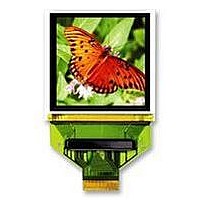
Manufacturer Part Number
DD-9664FC-2A
Description
DISPLAY, OLED, RGB, 96X64
Manufacturer
DENSITRON
Datasheet
1.DD-9664FC-2A.pdf
(29 pages)
Specifications of DD-9664FC-2A
Screen Size
24.13mm
Resolution
96 X 64
Viewing Area (h X W)
15.42mm X 22.14mm
Pixel Size (h X W)
0.19mm X 0.05mm
Voltage Rating
2.8V
External Depth
1.5mm
External Length / Height
22.2mm
External
RoHS Compliant
Svhc
No SVHC (15-Dec-2010)
Rohs Compliant
Yes
Connector Type
EVK-Connect
Interface Type
Parallel, Serial


3.3 INTERFACE PIN ASSIGNMENT
13~20
No.
10
11
12
4.
1
2
3
5
6
7
8
9
DENSITRON TECHNOLOGIES plc. – PROPRIETARY DATA – ALL RIGHTS RESERVED
Product No.
R/W#(WR#)
Symbol
VDDIO
E(RD#)
D0~D7
RES#
VDD
IREF
D/C#
N.C.
VSS
BS1
BS2
CS#
DD-9664FC-2A
I/O
I/O
P
P
P
I
I
I
I
I
I
-
I
Reserved Pin (Supporting Pin).
The supporting pins can reduce the influences from stresses on
the function pins.
Ground of System.
This is a ground pin. It also acts as a reference for the logic pins,
the OLED driving voltages and the analog circuits. It must be
connected to external ground.
Power Supply for Interface Logic Level.
This is a voltage supply pin. It must be connected to external
source.
Power Supply for Interface Logic Level.
It Should match with the MCU interface voltage level. VDDIO
must always be equal or lower than VDD
Communicating Protocol Select.
These pins are MCU interface selection input. See the following
table:
Current Reference for Brightness Adjustment.
This pin is segment current reference pin. A resistor should be
connected between this pin and VSS. Set the current at 10uA.
Chip Select.
This pin is the chip select input. The chip is enabled for MCU
communication only when CS# is pulled low.
Power Reset for Controller and Driver.
This pin is reset signal input. When the pin is low, initialization
of the chip executed.
Data/Command Control.
This pin is Data/Command control pin. When the pin is pulled
high, the input at D7~D0 is treated as display data. When the
pin is pulled low, the input at D7~D0 will be transferred to the
command register. For detail relationship to MCU interface
signal, please refer to the Timing Characteristics Diagrams.
Read/Write Select or Write.
This pin is MCU interface input. When interface to a 68XX-
series microprocessor, this pin will be used as the Read/Write
(R/W#) selection input. Pull this pin to “High” for read mode
and pull it to “Low” for write mode.
When 80XX interface mode is selected this pin will be the Write
(WR#) input. Data write operation is initiated when this pin is
pulled low and the CS# is pulled low.
Read/ Write Enable or Read.
This pin is MCU interface input. When interfacing to a 68XX-
series microprocessor this pin will be used as the Enable (E)
signal. Read/Write operation is initiated when this pin is pulled
high and the CS# is pulled low.
When connecting to an 80XX-microprocessor, this pin receives
the Read (RD#) signal. Data read operation is initiated when this
pin is pulled low and CS# is pulled low.
Host Data Input / Output Bus
These pins are 8 bit bi-directional data bus to be connected to
BS1
BS2
REV. A
REV.
68XX-parallel
0
1
Function
80XX-parallel
1
1
Page
Serial
0
0
9 / 29
Related parts for DD-9664FC-2A
Image
Part Number
Description
Manufacturer
Datasheet
Request
R

Part Number:
Description:
PMOLED, 96*16, BLUE
Manufacturer:
DENSITRON
Datasheet:
Part Number:
Description:
PMOLED, 96*39, BLUE
Manufacturer:
DENSITRON
Datasheet:
Part Number:
Description:
PMOLED, 96*64, BLUE
Manufacturer:
DENSITRON
Datasheet:
Part Number:
Description:
PMOLED, 96*64, WHITE
Manufacturer:
DENSITRON
Datasheet:
Part Number:
Description:
PMOLED, 96*16, BLUE
Manufacturer:
DENSITRON
Datasheet:

Part Number:
Description:
LCD MODULE, 128X240, YELLOW/GREEN
Manufacturer:
DENSITRON
Datasheet:

Part Number:
Description:
LCD MODULE, 128X240, BLUE
Manufacturer:
DENSITRON
Datasheet:
Part Number:
Description:
PMOLED, 128*128, COLOUR
Manufacturer:
DENSITRON
Datasheet:

Part Number:
Description:
DISPLAY, OLED, 128X32, BLUE
Manufacturer:
DENSITRON
Datasheet:
Part Number:
Description:
128 x 240 PIXEL INDUSTRIAL TOUCH MONITOR
Manufacturer:
Densitron Corporation
Part Number:
Description:
64 x 240 PIXEL INDUSTRIAL TOUCH MONITOR
Manufacturer:
Densitron Corporation
Part Number:
Description:
320 x 240 PIXEL INDUSTRIAL TOUCH MONITOR
Manufacturer:
Densitron Corporation
Part Number:
Description:
320 x 240 PIXEL INDUSTRIAL TOUCH MONITOR
Manufacturer:
Densitron Corporation
Part Number:
Description:
132 Seg / 65 Com Driver & Controller For Stn Lcd
Manufacturer:
Densitron Corporation
Datasheet: