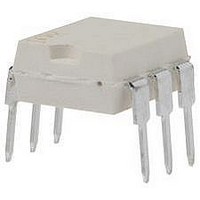
H11N1-M Fairchild Semiconductor, H11N1-M Datasheet - Page 3

H11N1-M
Manufacturer Part Number
H11N1-M
Description
OPTOCOUPLER, SCHMITT TRIGGER, 7500VRMS
Manufacturer
Fairchild Semiconductor
Datasheet
1.H11N1-M.pdf
(10 pages)
Specifications of H11N1-M
No. Of Channels
1
Optocoupler Output Type
Schmitt Trigger
Input Current
10mA
Output Voltage
16V
Opto Case Style
DIP
No. Of Pins
6
Isolation Voltage
7.5kV
Input Current Max
10mA
Rohs Compliant
Yes
Lead Free Status / RoHS Status
Lead free / RoHS Compliant
©2005 Fairchild Semiconductor Corporation
H11N1M, H11N2M, H11N3M Rev. 1.0.2
Electrical Characteristics
Individual Component Characteristics
Transfer Characteristics
Switching Speed
Isolation Characteristics
*Typical values at T
Notes:
1. Maximum I
2. H11N1: R
EMITTER
DETECTOR
I
V
C
R
Symbol
F(off)
Symbol
Symbol
Symbol
ISO
ISO
ISO
I
would require the LED to be driven at a current greater than 3.2mA to guarantee the device will turn on. A 10% guard band
is recommended to account for degradation of the LED over its lifetime. The maximum allowable LED drive current is 30mA.
CC(off)
I
V
CC(on)
I
I
I
V
C
t
t
V
F(on)
F(off)
I
OH
PHL
PLH
CC
R
F
t
t
J
OL
/ I
r
f
F(on)
E
Input Forward Voltage
Reverse Current
Capacitance
Operating Voltage Range
Supply Current
Output Current, High
F(ON)
Input-Output Isolation Voltage f = 60 Hz, t =1 sec.
Isolation Capacitance
Isolation Resistance
= 910 , H11N2: R
Supply Current
Output Voltage, Low
Turn-On Threshold Current R
Turn-Off Threshold Current R
Hysteresis Ratio
Propagation Delay Time
HIGH-to-LOW
Rise Time
Propagation Delay Time
LOW-to-HIGH
Fall Time
Data Rate
DC Characteristics
AC Characteristics
is the maximum current required to trigger the output. For example, a 3.2mA maximum trigger current
Parameters
A
= 25°C
Parameters
E
= 560 , H11N3: R
(T
A
= 25°C unless otherwise specified.)
I
I
V
V = 0, f = 1.0MHz
I
I
F
F
F
F
R
I
R
I
R
C = 120pF, t
R
C = 120pF, t
R
C = 120pF, t
R
C = 120pF, t
R
= 10mA
= 0.3mA
= 0, V
= 0.3mA, V
F
F
= 5V
L
L
L
L
E
E
E
E
= I
V
V
= 10mA, V
Test Conditions
=270 ,V
=270 , V
Test Conditions
Test Conditions
= 270 , V
= 270 , V
=
=
=
=
I-O
I-O
F(on)
(2)
(2)
(2)
(2)
CC
= 0V, f = 1 MHz
= ±500 VDC
, Figure 1
, Figure 1
, Figure 1
, Figure 1
E
= 5V
Test Conditions
= 240
max.
CC
CC
CC
P
P
P
P
CC
CC
CC
= 1µs,
= 1µs,
= 1µs,
= 1µs,
=5V,
= V
3
= 5V
= 5V
= 5V
= 5V
O
= 15V
(1)
H11N1M
H11N2M
H11N3M
Device
Device
Device
All
All
All
All
All
All
All
All
All
All
All
All
All
All
All
Min.
7500
10
Min.
0.75
11
Min.
Min.
0.65
0.8
2.3
4.1
0.3
4
Typ.*
Typ.*
0.4
1.25
Typ.*
Typ.*
1.4
100
150
6
6.5
7.5
12
5
Max.
Max.
100
100
Max.
Max.
0.6
10
15
10
0.95
330
330
0.5
3.2
2
10
10
www.fairchildsemi.com
5
Units
V
Units
Units
Units
PEAK
MHz
mA
pF
µA
µA
pF
mA
mA
mA
V
V
ns
ns
ns
ns
V


