H11B3 Vishay, H11B3 Datasheet - Page 2
H11B3
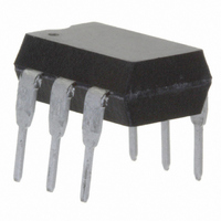
Manufacturer Part Number
H11B3
Description
OPTOCOUPLER, PHOTO DARLINGTON, 5300VRMS
Manufacturer
Vishay
Datasheet
1.H11B1.pdf
(7 pages)
Specifications of H11B3
No. Of Channels
1
Optocoupler Output Type
Photodarlington
Input Current
50mA
Output Voltage
30V
Opto Case Style
DIP
No. Of Pins
6
Mounting Type
Through Hole
Isolation Voltage
5.3kV
Number Of Channels
1
Input Type
DC
Voltage - Isolation
5300Vrms
Current Transfer Ratio (min)
100% @ 1mA
Voltage - Output
25V
Current - Output / Channel
100mA
Current - Dc Forward (if)
60mA
Vce Saturation (max)
1V
Output Type
Darlington with Base
Package / Case
6-DIP (0.300", 7.62mm)
Forward Current
60 mA
Maximum Input Diode Current
60 mA
Maximum Reverse Diode Voltage
3 V
Output Device
Darlington With Base
Configuration
1
Maximum Collector Emitter Voltage
30 V
Maximum Collector Emitter Saturation Voltage
1000 mV
Maximum Forward Diode Voltage
1.5 V
Maximum Collector Current
100 mA
Maximum Power Dissipation
260 mW
Maximum Operating Temperature
+ 100 C
Minimum Operating Temperature
- 55 C
Lead Free Status / RoHS Status
Lead free / RoHS Compliant
Current Transfer Ratio (max)
-
Lead Free Status / Rohs Status
Lead free / RoHS Compliant
Other names
H11B3GI
H11B3GI
H11B3VS
H11B3GI
H11B3VS
Available stocks
Company
Part Number
Manufacturer
Quantity
Price

Company:
Part Number:
H11B3
Manufacturer:
COOPER
Quantity:
5 510
Part Number:
H11B3
Manufacturer:
FAIRCHILD/仙童
Quantity:
20 000
Part Number:
H11B3SR2M
Manufacturer:
FAIRCHILD/仙童
Quantity:
20 000


H11B1, H11B2, H11B3
Vishay Semiconductors
Note
T
Stresses in excess of the absolute maximum ratings can cause permanent damage to the device. Functional operation of the device is not implied
at these or any other conditions in excess of those given in the operational sections of this document. Exposure to absolute maximum ratings for
extended periods of the time can adversely affect reliability.
Note
T
Minimum and maximum values were tested requierements. Typical values are characteristics of the device and are the result of engineering
evaluations. Typical values are for information only and are not part of the testing requirements.
www.vishay.com
284
amb
amb
ABSOLUTE MAXIMUM RATINGS
PARAMETER
COUPLER
Isolation test voltage
between emitter and detector
Creepage distance
Clearance distance
Comparative tracking index per
DIN IEC 112/VDE 0303, part 1
Isolation resistance
Total package dissipation (LED plus detector)
Derate linearly from 25 °C
Storage temperature
Operating temperature
Lead soldering time at 260 °C
ELECTRICAL CHARACTERISTCS
PARAMETER
INPUT
Forward voltage
Reverse current
Junction capacitance
OUTPUT
Collector emitter breakdown voltage
Collector base breakdown voltage
Collector emitter leakage current
COUPLER
Saturation voltage collector-emitter
Capacitance (input to output)
CURRENT TRANSFER RATIO
PARAMETER
DC current transfer ratio
Emitter collector breakdown voltage
= 25 °C, unless otherwise specified.
= 25 °C, unless otherwise specified.
For technical questions, contact: optocoupler.answers@vishay.com
I
I
V
C
V
I
E
I
V
TEST CONDITION
TEST CONDITION
C
C
CE
= 100 µA , I
CE
Optocoupler, Photodarlington
= 100µA, I
F
= 1 mA, I
= 1 mA, I
= 0 V, f = 1 MHz
= 10 V, I
= 5 V, I
I
I
F
F
V
with Base Connection
= 50 mA
= 10 mA
R
= 3 V
Output, High Gain,
F
F
C
F
F
V
F
V
= 1 mA
= 0 mA
= 1 mA
IO
= 0 mA
= 0 mA
= 0 mA
IO
= 500 V, T
TEST CONDITION
= 500 V, T
H11B1
H11B2
H11B3
amb
H11B1
H11B2
H11B3
PART
PART
amb
= 100 °C
= 25 °C
SYMBOL
SYMBOL
CTR
CTR
CTR
BV
BV
BV
V
I
C
CEO
CEsat
V
V
V
C
I
R
CEO
ECO
CBO
IO
F
F
F
j
DC
DC
DC
SYMBOL
V
T
MIN.
MIN.
CTI
R
R
T
500
200
100
P
amb
30
30
ISO
stg
7
IO
IO
tot
TYP.
TYP.
- 55 to + 150
- 55 to + 100
1.1
1.1
1.1
0.5
50
VALUE
≥ 10
≥ 10
5300
175
260
≥ 7
≥ 7
3.5
10
Document Number: 83609
12
11
MAX.
MAX.
100
1.5
1.5
1.5
Rev. 1.6, 10-Dec-08
10
1
mW/°C
UNIT
V
mW
mm
mm
°C
°C
RMS
Ω
Ω
s
UNIT
UNIT
µA
nA
pF
pF
%
%
%
V
V
V
V
V
V
V
Related parts for H11B3
Image
Part Number
Description
Manufacturer
Datasheet
Request
R

Part Number:
Description:
357-036-542-201 CARDEDGE 36POS DL .156 BLK LOPRO
Manufacturer:
Vishay
Datasheet:
Part Number:
Description:
357-036-542-201 CARDEDGE 36POS DL .156 BLK LOPRO
Manufacturer:
Vishay
Datasheet:
Part Number:
Description:
357-036-542-201 CARDEDGE 36POS DL .156 BLK LOPRO
Manufacturer:
Vishay
Datasheet:
Part Number:
Description:
357-036-542-201 CARDEDGE 36POS DL .156 BLK LOPRO
Manufacturer:
Vishay
Datasheet:
Part Number:
Description:
357-036-542-201 CARDEDGE 36POS DL .156 BLK LOPRO
Manufacturer:
Vishay
Datasheet:
Part Number:
Description:
357-036-542-201 CARDEDGE 36POS DL .156 BLK LOPRO
Manufacturer:
Vishay
Datasheet:
Part Number:
Description:
357-036-542-201 CARDEDGE 36POS DL .156 BLK LOPRO
Manufacturer:
Vishay
Datasheet:
Part Number:
Description:
357-036-542-201 CARDEDGE 36POS DL .156 BLK LOPRO
Manufacturer:
Vishay
Datasheet:
Part Number:
Description:
357-036-542-201 CARDEDGE 36POS DL .156 BLK LOPRO
Manufacturer:
Vishay
Datasheet:
Part Number:
Description:
357-036-542-201 CARDEDGE 36POS DL .156 BLK LOPRO
Manufacturer:
Vishay
Datasheet:
Part Number:
Description:
357-036-542-201 CARDEDGE 36POS DL .156 BLK LOPRO
Manufacturer:
Vishay
Datasheet:
Part Number:
Description:
357-036-542-201 CARDEDGE 36POS DL .156 BLK LOPRO
Manufacturer:
Vishay
Datasheet:
Part Number:
Description:
357-036-542-201 CARDEDGE 36POS DL .156 BLK LOPRO
Manufacturer:
Vishay
Datasheet:
Part Number:
Description:
357-036-542-201 CARDEDGE 36POS DL .156 BLK LOPRO
Manufacturer:
Vishay
Datasheet:
Part Number:
Description:
357-036-542-201 CARDEDGE 36POS DL .156 BLK LOPRO
Manufacturer:
Vishay
Datasheet: