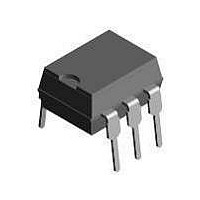
CNY17F-3X001 Vishay, CNY17F-3X001 Datasheet - Page 14

CNY17F-3X001
Manufacturer Part Number
CNY17F-3X001
Description
Optocoupler
Manufacturer
Vishay
Specifications of CNY17F-3X001
Leaded Process Compatible
Yes
Forward Current
60 mA
Maximum Input Diode Current
60 mA
Maximum Reverse Diode Voltage
6 V
Output Device
Transistor
Output Type
DC
Configuration
1
Input Type
DC
Maximum Collector Emitter Voltage
70 V
Maximum Collector Emitter Saturation Voltage
400 mV
Isolation Voltage
5300 Vrms
Current Transfer Ratio
200 %
Maximum Forward Diode Voltage
1.65 V
Maximum Collector Current
100 mA
Maximum Power Dissipation
150 mW
Maximum Operating Temperature
+ 100 C
Minimum Operating Temperature
- 55 C
Package / Case
PDIP-6
No. Of Channels
1
Optocoupler Output Type
Phototransistor
Input Current
60mA
Output Voltage
70V
Opto Case Style
DIP
No. Of Pins
6
Approval Bodies
UL, IEC65, IEC950, BS6301,
Rohs Compliant
Yes
Lead Free Status / RoHS Status
Lead free / RoHS Compliant
Lead Free Status / RoHS Status
Lead free / RoHS Compliant, Lead free / RoHS Compliant
Available stocks
Company
Part Number
Manufacturer
Quantity
Price
Option Information
Vishay Semiconductors
www.vishay.com
4
DESCRIPTION
Maximum permissible overvoltage (transient
overvoltage)
Partial discharge test voltage
Safety maximum ratings
(maximum permissible ratings in case of a fault,
also refer to diagram)
Package temperature
Current
(input current I
Derating with higher ambient temperature
Power (output or total power dissipation, T
Derating with higher ambient temperature
Insulation resistance at T
DESCRIPTION
Installation category (DIN VDE 0110)
For rated line voltages ≤ 300 V
For rated line voltages ≤ 600 V
For rated line voltages ≤ 1000 V
IEC climatic category (DIN IEC 60068 Part 1/9.80)
Pollution degree (DIN VDE 0110 Part 1/1.89)
Maximum operation insulating voltage
Test voltage input/output, procedure b
V
partial discharge < 5 pC
Test voltage input/output, procedure a
V
partial discharge < 5 pC
Maximum permissible overvoltage (transient
overvoltage)
Partial discharge test voltage
Safety maximum ratings
(maximum permissible ratings in case of a fault,
also refer to diagram)
Package temperature
Current
(input current I
Derating with higher ambient temperature
Power (output or total power dissipation, T
Derating with higher ambient temperature
Insulation resistance at T
Pr
Pr
= 1.875 x V
= 1.5 x V
IORM
F
F
IORM
, P
, P
, type and sampling Test t
Si
Si
, routine 100 % test, t
= 0, T
= 0, T
Si
Si
A
A
V
V
= 25 °C)
= 25 °C)
I/O
I/O
(1)
(1)
RMS
RMS
= 500 V
= 500 V
RMS
For technical questions, contact: optocoupler.answers@vishay.com
(1)
(1)
(1)
p
A
A
= 1 s,
p
= 25 °C)
= 25 °C)
= 60 s,
SYMBOL
SYMBOL
Option Information
V
V
V
V
V
ΔP
ΔP
INITIAL
INITIAL
DI
DI
P
R
V
V
P
R
IOTM
IORM
IOTM
T
T
I
I
si
si
Si
Pr
Pr
Si
si
IS
si
IS
Si
Si
Si
Si
SYSTEM 4
55/100/21
IL4116
IL4117
IL4118
IL4216
IL4217
IL4218
- 1.65
- 3.33
> 10
IL410
IL420
I - IV
1594
1275
6000
6000
I - III
850
175
250
500
2
9
(2)
SYSTEM 5
55/100/21
SYSTEM 2
SFH6135
SFH6136
SFH6138
SFH6139
SFH6345
6N135
6N136
6N138
6N139
- 3.33
> 10
> 10
- 2.67
- 4.67
1181
8000
8000
I - IV
I - IV
8000
8000
630
945
175
300
500
175
400
700
- 2
2
9
9
Document Number: 83713
IL300DEFG
SYSTEM 7
55/100/21
IL300EF
IL300E
IL300F
IL300
- 1.57
> 10
1669
1335
8000
8000
I - IV
I - IV
- 3.1
890
165
235
465
2
Rev. 1.7, 11-Sep-07
9
mW/K
mW/K
mA/K
UNIT
mA/K
mW
UNIT
mW
mA
mA
°C
W
°C
W
V
V
V
V
V
V
V


