SG-3030LC Epson Toyocom Corporation, SG-3030LC Datasheet
SG-3030LC
Manufacturer Part Number
SG-3030LC
Description
SPXO, 32.768KHZ, SMD
Manufacturer
Epson Toyocom Corporation
Series
SG-3030r
Datasheet
1.SG-3030JC.pdf
(2 pages)
Specifications of SG-3030LC
Operating Temperature Range
-40°C To +85°C
Load Capacitance
15pF
Resonator Case
SMD
No. Of Pins
6
Frequency Tolerance
-120ppm, +10ppm
Frequency
32.768kHz
Supply Voltage
1.5V To 5.5V
Oscillator Mounting
SMD
Rohs Compliant
Yes
Lead Free Status / RoHS Status
Lead free / RoHS Compliant
Available stocks
Company
Part Number
Manufacturer
Quantity
Price
Company:

Part Number:
SG-3030LC
Manufacturer:
EPSONTOYOCOM
Quantity:
50 000
Part Number:
SG-3030LC
Manufacturer:
EPSON/爱普生
Quantity:
20 000
Company:
Part Number:
SG-3030LC 32.768KHZ
Manufacturer:
EPSON
Quantity:
50 000
Part Number:
SG-3030LC 32.768000KHZ
Manufacturer:
EPSON/爱普生
Quantity:
20 000
Company:
Part Number:
SG-3030LCB
Manufacturer:
EPSON
Quantity:
2 777


Unless otherwise stated, characteristics (specifications) shown in the above table are based on the rated operating temperature and voltage condition.
Output frequency range
Supply voltage
Interface power supply voltage
Temperature
range
Frequency tolerance
Frequency temperature coefficient
Frequency / voltage coefficient
Current consumption
Symmetry
High output voltage
Low output voltage
Output load condition (CMOS)
Output rise and fall time
Oscillation start up time
Frequency aging
CRYSTAL OSCILLATOR
32.768 kHz
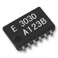
SG - 3030LC
SG - 3040LC
SG - 3032JC
Block diagram (SG-3030LC
External dimension
Footprint (Recommended)
Built-in 32.768 kHz crystal unit allows adjustment-free efficient operation..
Use of C-MOS IC enables reduction of current consumption.
VIO controls swing amplitude (SG-3030 / SG-3040).
Specifications (characteristics)
32 .76 8 k Hz
SG-3030LC
22
SG-3030LC
# 1
# 12
E 3040
0.5
V
3.6
A123B
C C
Crystal oscillator
Crystal oscillator
Crystal oscillator
Crystal oscillator
Storage temperature
Operating temperature
0.22
0.2
Item
/
# 7
# 6
3040LC
/
3040LC
0 Min.
( 0.4 )
V
Pin map
Pin
1
2
3
4
5
6
I
V
N.C.
N.C.
N.C.
N.C.
GND
Connection
2.8
IO
0.5
V
2.77
2.5
O
0.2
C
C
/
/
Pin
12
11
10
G
9
8
7
D
JF
JC
F_tol(osc)
0.27
R
L_CMOS
F_aging
Symbol
F
T_use
F
T_stg
D
Connection
V
N.C.
N.C.
N.C.
N.C.
OUT
SYM
O
t
t
V
V
V
O
CC
V
I
r
OSC
Metal may be exposed on the top or bottom of this product. This will not affect any quality, reliability or electrical spec.
f
-V
CC
CC
-T
OH
OL
/
0
IO
/
V
t
JC
CC
C
f
C O R E
/
R
JC
/
F
JF,SG3040JC
SG-3030LC
2
0.4
1.5 V to 5.5 V
1.5 V to 5.5 V
200 ns Max.
SG-3030JF
2 A Max.
1 s Max.
10
#4
#1
http://www.epsontoyocom.co.jp
SG3030 B
E 9245A
7.1 0.2
-6
/ V Max.
5.08
-40 C to +85 C
/
JF
V
45 % to 55 %
SG-3030JF
IO
#3
/
#2
-0.4 V Min.
JC
0 Min.
+10
/
LC)
5
-55 C to +125 C
SG-3040LC
Specifications
5
(0.75)
0.9 V to 3.6 V
0.9 V to 3.6 V
5 23
32.768 kHz
15 pF Max.
0.4 V Max.
3.1 A Max.
10
10
10
-6
-6
/ year Max.
Pin map
/ -120
-6
5.08
Actual size
Pin
1
2
3
4
/ V Max.
10
LC Type.
Connection
V
GND
OUT
V
-6
/
100 ns Max.
IO
CC
JC
SG-3030LC
SG-3040LC
3 s Max.
10
1.8
O U T
V
G N D
(0.75)
-6
IO
-20 C to +70 C
2
V
1.8 V to 3.6 V
40 % to 60 %
SG-3032JC
CC
5 A Max
10
-0.4 V Min.
-
-6
/ V Max. +25 C
0.51
SG-3030JC
If no t use V
JF Type.
SG3030 B
E
#1
#4
10.5 Max.
SG-3030JF
8123A
5.08
Store as bare product after unpacking
+25 C,V
-20 C to +70 C (+25 C is reference)
3.3 V, No load condition
1/2 V
I
I
CMOS load
CMOS load:20 % V
(SG-3040: V
Time at minimum Supply voltage to be 0 s
+25 C (SG-3030: V
+25 C, V
OH
OL
/
3040JC
= 0.4 mA
=-0.4 mA (SG-3040: V
SG-3030JC
#3
#2
IO
CC
(V
function , co nne ct #1 to V
0.05Min.
/
CC
3032JC
CC
IO
=3.3 V (SG-3040: V
)level (SG-3040: V
= 3.3 V, First year
IO
JC Type.
=1.2 V to 3.6 V)
(SG-3040: V
/
3040JC
(1.0)
CC
CC
Remarks
(V
5.08
= 2.0 V to 5.5 V)
Pin
1
2
3
4
IO
/
3032JC
) to 80 % V
SG-3030JC
SG-3040JC
SG-3032JC
SG-3030
SG-3040
3.6
IO
IO
V
=1.2 V to 3.6 V)
Connection
IO
=1.2 V to 3.6 V)
IO
CC
GND
OUT
V
=1.2 V to 3.6 V)
CC
1.3
=1.2 V)
SG-3032
(1.0)
N.C.
CC
C C
(Unit:mm)
(Unit:mm)
(V
.
IO
)level
Related parts for SG-3030LC
Image
Part Number
Description
Manufacturer
Datasheet
Request
R

Part Number:
Description:
OSCILLATOR 60.000MHZ PDIP
Manufacturer:
Epson Toyocom Corporation

Part Number:
Description:
OSCILLATOR 20.0000MHZ SMD
Manufacturer:
Epson Toyocom Corporation
Datasheet:
Part Number:
Description:
OSCILLATOR 1.8432MHZ SMD
Manufacturer:
Epson Toyocom Corporation
Datasheet:
Part Number:
Description:
OSCILLATOR 2.4576MHZ SMD
Manufacturer:
Epson Toyocom Corporation
Datasheet:
Part Number:
Description:
OSCILLATOR 3.6864MHZ SMD
Manufacturer:
Epson Toyocom Corporation
Datasheet:
Part Number:
Description:
OSCILLATOR 18.4320MHZ SMD
Manufacturer:
Epson Toyocom Corporation
Datasheet:
Part Number:
Description:
OSCILLATOR 6.0000MHZ SMD
Manufacturer:
Epson Toyocom Corporation
Datasheet:
Part Number:
Description:
OSCILLATOR 10.0000MHZ SMD
Manufacturer:
Epson Toyocom Corporation
Datasheet:
Part Number:
Description:
OSCILLATOR 16.0000MHZ SMD
Manufacturer:
Epson Toyocom Corporation
Datasheet:
Part Number:
Description:
OSCILLATOR 24.0000MHZ SMD
Manufacturer:
Epson Toyocom Corporation
Datasheet:

Part Number:
Description:
IC, RTC, FULL CALENDAR, VSOJ-20
Manufacturer:
Epson Toyocom Corporation
Datasheet:

Part Number:
Description:
IC, RTC, GREGORIAN CALENDAR, DIP-18
Manufacturer:
Epson Toyocom Corporation
Datasheet:
Part Number:
Description:
IC, RTC, GREGORIAN CALENDAR, SOIC-24
Manufacturer:
Epson Toyocom Corporation
Datasheet:

Part Number:
Description:
IC REAL TIME CLOCK 14-SOIC
Manufacturer:
Epson Toyocom Corporation
Datasheet:

Part Number:
Description:
IC REAL TIME CLOCK 14PIN-SOP
Manufacturer:
Epson Toyocom Corporation
Datasheet:
SG-3030LC Summary of contents
Page 1
... Low output voltage V OL Output load condition (CMOS) L_CMOS t t Output rise and fall time / Oscillation start up time OSC Frequency aging F_aging Unless otherwise stated, characteristics (specifications) shown in the above table are based on the rated operating temperature and voltage condition. Block diagram (SG-3030LC . ...
Page 2
... LAN and WAN on a global scale. Epson Toyocom Corporation addresses every single aspect within a network environment. The new corporation offers “Digital Convergence” solutions to problems arising with products for consumer use, such as, core network systems and automotive systems ...