EVAL-AD7747EBZ Analog Devices Inc, EVAL-AD7747EBZ Datasheet - Page 23
EVAL-AD7747EBZ
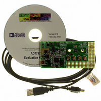
Manufacturer Part Number
EVAL-AD7747EBZ
Description
24-Bit Capacitance-to-Digital Converter Eval. Board
Manufacturer
Analog Devices Inc
Specifications of EVAL-AD7747EBZ
Silicon Manufacturer
Analog Devices
Application Sub Type
Capacitance-to-Digital Converter
Kit Application Type
Data Converter
Silicon Core Number
AD7747
Sensor Type
Touch, Capacitive
Interface
I²C
Voltage - Supply
2.7 V ~ 5.25 V
Embedded
No
Utilized Ic / Part
AD7747
Kit Contents
Board
Rohs Compliant
Yes
Lead Free Status / RoHS Status
Lead free / RoHS Compliant
Sensitivity
-
Sensing Range
-
Lead Free Status / RoHS Status
Lead free / RoHS Compliant, Lead free / RoHS Compliant
Available stocks
Company
Part Number
Manufacturer
Quantity
Price
Company:

Part Number:
EVAL-AD7747EBZ
Manufacturer:
Analog Devices Inc
Quantity:
135


PARASITIC CAPACITANCE
The CDC architecture used in the AD7747 measures the
capacitance C
Most applications use the active shield to avoid external influ-
ences during the CDC. However, any parasitic capacitance, C
as shown in Figure 33, can affect the CDC result.
A parasitic capacitance, C
ground adds directly to the value of the capacitance C
therefore, the CDC result is: DATA ≈ C
bration might be sufficient to compensate for a small parasitic
capacitance (C
CAPDAC can be used to compensate, followed by an offset
calibration to ensure the full range of ±8pF is available for
the system.
Other parasitic capacitances, such as C
and ground as well as C
could influence the conversion result. However, the graphs in
the Typical Performance Characteristics section show that the
effect of parasitic capacitance of type C
insignificant to the CDC result. Figure 7 and Figure 8 show the
gain error caused by C
by C
PARASITIC RESISTANCE
C
R
(17pF ± 8pF)
9 TO 25pF
P1
P1
C
P3
X
.
Figure 32. Using CAPDAC in Differential Configuration
C
C
X
X
X
C
17pF
P1
connected between the CIN pin and ground.
Y
Figure 34. Parasitic Resistance on CIN
≤ 1pF). For a larger parasitic capacitance, the
C
R
Figure 33. Parasitic Capacitance
P2
P2
CIN(+)
CIN(–)
SHLD
P2
P3
. Figure 9 shows the gain error caused
P1
between the CIN pin and SHLD,
C
R
, coupled in between CIN and
P3
SHLD
P3
SHLD
CAPDIFF = 1
CAPDAC(+)
17pF
CAPDAC(–)
17pF
CIN
CIN
P2
P2
X
/C
+ C
between active shield
P3
P1
below 250 pF is
. An offset cali-
±8pF
CDC
CDC
CDC
0xFFFFFF
0x000000
X
TO
DATA
and,
DATA
DATA
Rev. 0 | Page 23 of 28
P
,
Parasitic resistances, as shown in Figure 34, cause leakage
currents, which affect the CDC result. The AD7747 CDC
measures the charge transfer between the CIN pin and ground.
Any resistance connected in parallel to the measured
capacitance, C
transfers charge. Therefore, the parallel resistor is seen as an
additional capacitance in the output data. A resistance in the
range of R
An offset calibration can be used to compensate for the effect of
small leakage currents. A higher leakage current to ground,
R
nonlinearity error. See Figure 10 in the Typical Performance
Characteristics section.
A parasitic resistance, R
as R
Figure 34, cause a leakage current, which affects the CDC result
and is seen as an offset in the data. An offset calibration can be
used to compensate for effect of the small leakage current
caused by a resistance R
Figure 12, and Figure 13 in the Typical Performance
Characteristics section.
PARASITIC SERIAL RESISTANCE
The AD7747 CDC result is affected by a resistance in series
with the measured capacitance. The serial resistance should be
less than 10 kΩ for the specified performance. See Figure 14 in
the Typical Performance Characteristics section.
CAPACITIVE GAIN CALIBRATION
The AD7747 gain is factory calibrated for the full scale of
±8.192 pF in the production for each part individually. The
factory gain coefficient is stored in a one-time programmable
(OTP) memory and is copied to the capacitive gain register at
power-up or after reset.
The gain can be changed by executing a capacitance gain calibra-
tion mode, for which an external full-scale capacitance needs
to be connected to the capacitance input, or by writing a user
value to the capacitive gain register. This change would be only
temporary, and the factory gain coefficient would be reloaded
back after power-up or reset. The part is tested and specified for
use only with the default factory calibration coefficient.
P1
C
≤ 10 MΩ, results in a gain error, an offset error, and a
P3
X
between the CIN pin and the active shield, as shown in
R
S
P1
≥ 10 MΩ causes an offset error in the CDC result.
X
, such as the parasitic resistance, R
Figure 35. Parasitic Serial Resistance
P2
P2
SHLD
, between SHLD and ground, as well
and R
CIN
P3
≥ 200 kΩ. See Figure 11,
CDC
P1
, also
AD7747
DATA
Related parts for EVAL-AD7747EBZ
Image
Part Number
Description
Manufacturer
Datasheet
Request
R


Part Number:
Description:
BOARD EVAL FOR SI270X-A
Manufacturer:
Silicon Laboratories Inc
Datasheet:

Part Number:
Description:
BUCK CONV REF DESIGN KIT IP1201
Manufacturer:
International Rectifier
Datasheet:
Part Number:
Description:
BOARD DEMO SYNC DUAL BUCK CNVTER
Manufacturer:
International Rectifier
Datasheet:
Part Number:
Description:
BOARD DEMO SYNC BUCK CONVETER
Manufacturer:
International Rectifier
Datasheet:

Part Number:
Description:
EVALBOARD/EB Omnidirectional microphone - Analog
Manufacturer:
Analog Devices
Datasheet:
Part Number:
Description:
EVALBOARD/EB Omnidirectional microphone - Analog
Manufacturer:
Analog Devices
Datasheet:


Part Number:
Description:
BOARD EVAL LED DRIVER LT3756
Manufacturer:
Linear Technology
Datasheet:

Part Number:
Description:
BOARD EVAL FOR AD7741/7742
Manufacturer:
Analog Devices Inc
Datasheet:

Part Number:
Description:
±1.7g Dual-Axis IMEMS Accelerometer Evaluation Board
Manufacturer:
Analog Devices Inc
Datasheet:

Part Number:
Description:
IC MULTIPLIER ANALOG 8-SOIC T/R
Manufacturer:
Analog Devices Inc
Datasheet:

Part Number:
Description:
IC ANALOG MULTIPLIER 8-DIP
Manufacturer:
Analog Devices Inc
Datasheet:
Part Number:
Description:
IC ANALOG MULTIPLIER 8-SOIC
Manufacturer:
Analog Devices Inc
Datasheet:
Part Number:
Description:
IC ANALOG MULTIPLIER 8-DIP
Manufacturer:
Analog Devices Inc
Datasheet: