IRPP3637-18A International Rectifier, IRPP3637-18A Datasheet - Page 3
IRPP3637-18A
Manufacturer Part Number
IRPP3637-18A
Description
POWIR+ Chipset
Manufacturer
International Rectifier
Datasheet
1.IRPP3637-06A.pdf
(14 pages)
Specifications of IRPP3637-18A
Silicon Manufacturer
International Rectifier
Silicon Core Number
IR3637ASPBF
Kit Application Type
Power Management - Voltage Regulator
Application Sub Type
Synchronous Buck Controller
Lead Free Status / RoHS Status
Lead free / RoHS Compliant


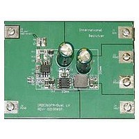
The 5V input power is connected
between terminals J1 and J2 and the
1.25V, 6A output power is obtained
through terminals J3 and J4.
The V
driver and high side driver power input
pins respectively. The V
includes the housekeeping power of the
PWM
lockout (UVLO) feature is associated
with each of these pins, which is set to
4.2V for V
pump circuit comprised of C13, D1, and
C14 applies approximately twice the
input voltage to the V
driving capability, hence reducing the
switching losses of the control FET
(Q1).
Upon application of the input power, the
output starts ramping up to regulation
within 4ms. The ramping time can be
adjusted through the soft start capacitor
C5.
synchronous buck regulator is set to
1.25V using the internal 0.8V reference
voltage.
The following equations are used to
calculate the MOSFET power loss.
Refer to the IRF8910PBF datasheet to
select the parametric values of the
power loss equations terms.
Control FET Losses:
Eq (1):
Synchronous FET Losses:
Eq (2):
Deadtime losses:
Eq (3):
www.irf.com
P
P
P
Q
Q
td
1
2
=
=
=
I
I
Q
Q
V
1
2
rms
CC
rms
SD
Start-Up Procedure
controller.
The
.
2
2
I
.
and V
R
.
R
o
CC
DQ
.
DQ
t
1
d
.
2
R
.
and 3.3V for V
.
R
F
Dn
output
Dn
sw
C
+
+
(
I
⎛
⎜
⎜
⎝
pins are the low side
o
Q
.
Q
ossQ
I
2
An
sw
g
1
C
1
2
.
voltage
V
.
V
pin to allow fast
in
in
+
+
under-voltage
Q
CC
Q
gQ
C
gQ
1
. A charge
.
V
2
.
V
dd
pin also
dd
+
of
+
Q
Q
ossQ
rrQ
1
the
.
2
V
RD-0604
.
V
in
in
).
⎞
⎟
⎟
⎠
F
.
SW
F
SW
Total FET losses:
Eq (4):
Where,
I
control and sync FETs respectively, in
Amps
I
R
R
temperature
IRF8910PBF datasheet.
Q
V
converter
Q
V
4.5V.
I
Q
Q
reverse recovery charge in nC
V
forward voltage drop in volts. F
switching frequency of the sync buck
converter in hertz.
td is the dead time caused by the PWM
controller IC in seconds. This parameter
is specified in IR3637ASPBF datasheet.
For
programming the output voltage and the
soft start time, selection of input/output
capacitors and output inductor and
control loop compensation, refer to the
guidelines outlined in the IR3637ASPBF
PWM controller datasheet.
IR's online design tool POWIR
be used to customize a design for
applications outside the standard 4.5V
to 5.5V input range and 1.25V output,
and for varied design goal objectives.
P
Q1rms
O
g
IN
dd
SD
FET
D
Dn
SW
g
OSS
rr
is the drive current which is 0.25A.
is the output load current in Amps
is the total gate charge in nC.
is the R
is the sync FET internal body diode
is the input voltage of the sync buck
is the sync FET internal body diode
is the FET drive voltage, which is
_
is the normalized R
is the FET switch charge in nC
total
is the FET output charge in nC.
and I
design
=
Q2rms
P
DSON
Q
1
+
calculations
in ohms of the FETs and
are the rms currents for
extracted
P
Q
2
+
P
td
DSON
from
related
factor vs
+
SW
3
should
is the
the
to
Related parts for IRPP3637-18A
Image
Part Number
Description
Manufacturer
Datasheet
Request
R

Part Number:
Description:
KIT REF DES 12A 1PH SYNC BUCK
Manufacturer:
International Rectifier
Datasheet:

Part Number:
Description:
BOARD REF DESIGN POWIR+
Manufacturer:
International Rectifier
Datasheet:

Part Number:
Description:
SCHOTTKY RECTIFIER
Manufacturer:
International Rectifier Corp.
Datasheet:
Part Number:
Description:
SCHOTTKY RECTIFIER
Manufacturer:
International Rectifier Corp.
Datasheet:
Part Number:
Description:
SCHOTTKY RECTIFIER
Manufacturer:
International Rectifier Corp.
Datasheet:
Part Number:
Description:
SCHOTTKY RECTIFIER
Manufacturer:
International Rectifier Corp.
Datasheet:
Part Number:
Description:
SCHOTTKY RECTIFIER
Manufacturer:
International Rectifier Corp.
Datasheet:
Part Number:
Description:
SCHOTTKY RECTIFIER
Manufacturer:
International Rectifier Corp.
Datasheet:
Part Number:
Description:
SCHOTTKY RECTIFIER
Manufacturer:
International Rectifier Corp.
Datasheet:
Part Number:
Description:
SCHOTTKY RECTIFIER
Manufacturer:
International Rectifier Corp.
Datasheet:
Part Number:
Description:
SCHOTTKY RECTIFIER
Manufacturer:
International Rectifier Corp.
Datasheet:
Part Number:
Description:
SCHOTTKY RECTIFIER
Manufacturer:
International Rectifier Corp.
Datasheet:
Part Number:
Description:
SCHOTTKY RECTIFIER
Manufacturer:
International Rectifier Corp.
Datasheet:
Part Number:
Description:
SCHOTTKY RECTIFIER
Manufacturer:
International Rectifier Corp.
Datasheet:
Part Number:
Description:
SCHOTTKY RECTIFIER
Manufacturer:
International Rectifier Corp.
Datasheet: