CDK5560 Cirrus Logic Inc, CDK5560 Datasheet - Page 17
CDK5560
Manufacturer Part Number
CDK5560
Description
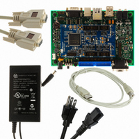
KIT - CDB5560 W/ Capture Plus II System
Manufacturer
Cirrus Logic Inc
Series
CapturePLUS™IIr
Specifications of CDK5560
Number Of Adc's
1
Number Of Bits
24
Sampling Rate (per Second)
50k
Data Interface
Serial
Inputs Per Adc
1 Differential
Input Range
±3 V
Power (typ) @ Conditions
90mW @ 2.5 V
Voltage Supply Source
Dual ±
Operating Temperature
-40°C ~ 85°C
Utilized Ic / Part
CS5560
Lead Free Status / RoHS Status
Contains lead / RoHS non-compliant
Other names
598-1277
CDK5560-1
CDK5560-1


3.6 Typical Connection Diagrams
The following figure depicts the CS5560 powered from bipolar analog supplies, +2.5 V and - 2.5 V.
DS713PP2
R
R
1
1
C
C
1
1
Figure 6. CS5560 Configured Using ± 2.5V Analog Supplies
Reference
(NOTE 1)
47pF
47pF
Voltage
4.99k
4.99k
+4.096
4.99k
4.99k
+2.5 V
-2.5 V
49.9
49.9
+2.048 V
+2.048 V
-2.048 V
-2.048 V
0 V
0 V
10 µF
(V+) Buffers On
(V-) Buffers Off
5/4/09
4700pF
4700pF
0.1 µF
C0G
C0G
0.1 µF
NOTES
1. See Section 3.3 Voltage Reference for information on required
2.Locate capacitors so as to minimize loop length.
3. The ±2.5 V supplies should also be bypassed to ground at the converter.
4. VLR and the power supply ground for the ±2.5 V should be
5. SCLK and SDO may require pull-down resistors in some applications.
6. An RC input filter can be used to band limit the input to reduce noise.
+2.5 V
-2.5 V
voltage reference performance criteria.
connected to the same ground plane under the chip.
Select R to be equal to the parallel combination of the feedback of the
feedback resistors 4.99k || 4.99k = 2.5k÷ ÷
BUFEN
VREF+
VREF-
AIN-
AIN+
0.1 µF
10
10
0.1 µF
X7R
V1+
V2+
V2-
DCR
V1-
CS5560
VLR2
SMODE
VLR
SLEEP
+3.3 V to +1.8 V
5
BP/UP
CONV
MCLK
SCLK
5
VL
SDO
RDY
RST
TST
CS
0.1 µF
50
CS5560
17
Related parts for CDK5560
Image
Part Number
Description
Manufacturer
Datasheet
Request
R

Part Number:
Description:
Development Kit
Manufacturer:
Cirrus Logic Inc
Datasheet:
Part Number:
Description:
Development Kit
Manufacturer:
Cirrus Logic Inc
Datasheet:


Part Number:
Description:
High-efficiency PFC + Fluorescent Lamp Driver Reference Design
Manufacturer:
Cirrus Logic Inc
Datasheet:
Part Number:
Description:
Development Kit
Manufacturer:
Cirrus Logic Inc
Datasheet:
Part Number:
Description:
Development Kit
Manufacturer:
Cirrus Logic Inc
Datasheet:

Part Number:
Description:
Development Kit
Manufacturer:
Cirrus Logic Inc
Datasheet:
Part Number:
Description:
Development Kit
Manufacturer:
Cirrus Logic Inc
Datasheet:
Part Number:
Description:
Development Kit
Manufacturer:
Cirrus Logic Inc
Datasheet:
Part Number:
Description:
Development Kit
Manufacturer:
Cirrus Logic Inc
Datasheet:

Part Number:
Description:
EVALUATION BOARD FOR CS8427
Manufacturer:
Cirrus Logic Inc
Datasheet:

Part Number:
Description:
BOARD EVAL FOR CS8416 RCVR
Manufacturer:
Cirrus Logic Inc
Datasheet:

Part Number:
Description:
EVALUATION BOARD FOR CS8420
Manufacturer:
Cirrus Logic Inc
Datasheet:

Part Number:
Description:
KIT DEVELOPMENT EP9315 ARM9
Manufacturer:
Cirrus Logic Inc
Datasheet:

Part Number:
Description:
KIT DEVELOPMENT EP9302 ARM9
Manufacturer:
Cirrus Logic Inc
Datasheet: