CRCW1206-KIT-102B S51 Vishay, CRCW1206-KIT-102B S51 Datasheet - Page 6
CRCW1206-KIT-102B S51
Manufacturer Part Number
CRCW1206-KIT-102B S51
Description
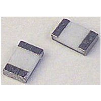
RESISTOR THICK FILM CHIP KIT, 250mW
Manufacturer
Vishay
Series
CRCWr
Datasheet
1.CRCW04023R00FKED.pdf
(8 pages)
Specifications of CRCW1206-KIT-102B S51
Kit Contents
For Use With
Range Of Resistor Values
1ohm To 10Mohm
Termination Type
SMD
Peak Reflow Compatible (260 C)
No
Filter Terminals
SMD
Leaded Process Compatible
No
Rohs Compliant
No
For Use With
CRCW1206
Lead Free Status / RoHS Status
Contains lead / RoHS non-compliant


D/CRCW e3
Vishay
www.vishay.com
130
THE PRODUCT DESCRIBED HEREIN AND THIS DATASHEET ARE SUBJECT TO SPECIFIC DISCLAIMERS, SET FORTH AT
TEST PROCEDURES AND REQUIREMENTS
EN
60115-1
CLAUSE
4.5
4.7
4.13
4.17.2
4.8.4.2
4.32
4.33
4.19
4.23
4.23.2
4.23.3
4.23.4
4.23.5
4.23.6
4.23.7
4.25.1
METHOD
60068-2
21 (Uu
21 (Uu
14 (Na)
30 (Db)
30 (Db)
58 (Td)
13 (M)
2 (Ba)
1 (Aa)
TEST
IEC
-
-
-
-
-
-
-
3
1
)
)
Short time overload
Substrate bending
Climatic sequence:
Rapid change of
Damp heat, cyclic
Damp heat, cyclic
Low air pressure
Voltage proof
Temperature
Solderability
temperature
Resistance
Endurance
(adhesion)
coefficient
DC load
at 70 °C
Dry heat
Shear
TEST
Cold
For technical questions, contact:
Standard Thick Film Chip Resistors
Stability for product types:
RR 1608 and smaller: 9 N
RR 2012 and larger: 45 N
This datasheet is subject to change without notice.
1 kPa; (25 ± 10) °C; 1 h
U =
duration: Acc. to style
Solder bath method;
Solder bath method;
U = 2.5 x
(20/- 55/20) C and
U = 1.4 x U
non activated flux;
non-activated flux;
30 min. at - 55 °C;
55 °C; 90 % RH;
55 °C; 90 % RH;
1.5 h on; 0.5 h off;
30 min. at 125 °C
Sn96.5Ag3Cu0.5
(20/125/20) C
PROCEDURE
U =
24 h; 5 cycles
70 °C; 1000 h
70 °C; 8000 h
Depth 2 mm;
125 °C; 16 h
24 h; 1 cycle
(235 ± 5) °C
(245 ± 5) C
1000 cycles
2 x U
- 55 °C; 2 h
P
Sn60Pb40
(2 ± 0.2) s
(3 ± 0.3) s
5 cycles
70
3 times
P
x R
D/CRCW e3
-
-
70
P
max.
ins
70
x R
U
; 60 s
;
x R
max.
;
thickfilmchip@vishay.com
±0.25 % R + 0.05)
± (0.25 % R + 0.05 )
± (1 % R + 0.05 )
± (1 % R + 0.05 )
± (1 % R + 0.05 )
± (2 % R + 0.1 )
No visible damage, no open circuit in bent position
OR BETTER
± 100 ppm/K
STABILITY
CLASS 1
± 1 %
PERMISSIBLE CHANGE (R)
Good tinning ( 95 % covered)
Good tinning ( 95 % covered)
No flashover or breakdown
± (0.25 % R + 0.05 )
SIZE 0402 to 2512
No visible damage
REQUIREMENTS
no visible damage
no visible damage
1 to 10 M
± (0.5 % R + 0.05 )
±0.5 % R + 0.05)
Document Number: 20035
www.vishay.com/doc?91000
± (1 % R + 0.05 )
± (2 % R + 0.1 )
± (2 % R + 0.1 )
± (4 % R + 0.1 )
OR BETTER
± 200 ppm/K
STABILITY
CLASS 2
Revision: 08-Mar-11
± 5 %