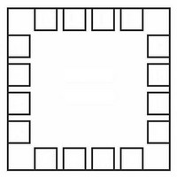
LDS8845002T2 Leadis Technology, LDS8845002T2 Datasheet

LDS8845002T2
Specifications of LDS8845002T2
Related parts for LDS8845002T2
LDS8845002T2 Summary of contents
Page 1
... DESCRIPTION The LDS8845 is a high efficiency ultra-low dropout current regulator that can drive up to four LEDs. The TYPICAL APPLICATION CIRCUIT © 2008 Leadis Technology Characteristics subject to change without notice LED current is easily adjustable by an external resistor per channel. The CTRL0 and CTRL1 logic inputs function as a LED enable and a PWM mode LED brightness control ...
Page 2
... Logic Level Threshold PWM frequency PWM duty cycle Thermal Shutdown Thermal Hysteresis Under Voltage Lockout (UVLO) Threshold *) Voltage drop at led pin, at which LED current falls 10% below set value © 2008 Leadis Technology Characteristics subject to change without notice Rating -0 -0 0.7V IN -65 to +150 ...
Page 3
... OFF 0 1 OFF OFF OFF TYPICAL CHARACTERISTICS V = 3.6V 104 mA (4 LEDs each OUT Power Efficiency vs. Input Voltage LED Current vs. Input Voltage © 2008 Leadis Technology Characteristics subject to change without notice LED2 LED1 OFF OFF = µ 3 OUT LED Current vs. Temperature EN V OUT I ...
Page 4
... LEDs) 50 mA/div PWM Mode (10 kHz, 50 Duty Cycle) CRL0 V OUT I LED (4 LEDs) 50 mA/div I Current vs. Duty Cycle LED © 2008 Leadis Technology Characteristics subject to change without notice PWM Mode (1 kHz, 50 Duty Cycle) CRL0 V OUT I LED (4 LEDs) 50 mA/div PWM Mode (50 kHz, 50 Duty Cycle) CRL0 V ...
Page 5
... V to 5.5 V. Whenever the input supply falls below the under-voltage threshold (2.2 V), all the LED channels are disabled, and the device enters shutdown mode. © 2008 Leadis Technology Characteristics subject to change without notice Function V is the driver output. Connect it to the LED OUT anodes ...
Page 6
... SET LED R SET its resistance. R value for typical I current is shown at the SET LED table below. © 2008 Leadis Technology Characteristics subject to change without notice Figure 2. LDS8845 Functional Block Diagram ILED The average current value may be decreased using PWM signal applied to either CTRL0 or CTRL1 pin. ...
Page 7
... Figure 3. Application circuit with three LEDs Figure 4. Application circuit with two LEDs Figure 5. Application circuit with two LEDs © 2008 Leadis Technology Characteristics subject to change without notice . OUT with accordingly Figure 6 ...
Page 8
... A copper area matching the TQFN exposed pad (PAD) must be connected to the ground plane underneath. The use of multiple via improves the package heat dissipation. Figure 7. Recommended layout © 2008 Leadis Technology Characteristics subject to change without notice 8 Doc. No. 8845DS, Rev. 1.5 ...
Page 9
... L 0.325 0.375 m 0.150 typ n 0.225 typ Note: 1. All dimensions are in millimeters 2. Complies with JEDEC Standard MO-220 © 2008 Leadis Technology Characteristics subject to change without notice MAX 0.80 0.05 0.228 0.30 3.05 1.75 3.05 1.75 0.425 9 Doc. No. 8845DS, Rev. 1.5 ...
Page 10
... E1 2.35 2.40 e 0.65 typ L 0.55 0.60 Note: 3. All dimensions are in millimeters 4. Complies with JEDEC Standard MO-220 © 2008 Leadis Technology Characteristics subject to change without notice MAX 0.80 0.05 0.228 0.38 4.10 2.45 4.10 2.45 0.65 10 Doc. No. 8845DS, Rev. 1.5 ...
Page 11
... The device used in the above example is a LDS8845 002–T2 ( 3x3 TQFN, Tape & Reel, 32/25/10.5 mA maximum current per LED bank). 4) For additional package and temperature options, please contact your nearest Leadis Technology Sales office. © 2008 Leadis Technology Characteristics subject to change without notice ...
Page 12
... Leadis Technology products are not designed, intended, or authorized for use as components in systems intended for surgical implant into the body, or other applications intended to support or sustain life, or for any other application in which the failure of the Leadis Technology product could create a situation where personal injury or death may occur. Leadis Technology reserves the right to make changes to or discontinue any product or service described herein without notice. Products with data sheets labeled " ...


