M0224SD-242MDBR1-1 Newhaven Display, M0224SD-242MDBR1-1 Datasheet
M0224SD-242MDBR1-1
Specifications of M0224SD-242MDBR1-1


Related parts for M0224SD-242MDBR1-1


M0224SD-242MDBR1-1 Summary of contents
Page 1
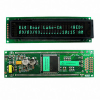
... M0224SD 242MDBR1 1 Vacuum Fluorescent Display Module RoHS Compliant nhtech@newhavendisplay.com Newhaven Display International, Inc. 2511 Technology Drive, Suite 101 Elgin IL, 60124 Ph: 847 844 8795 Fax: 847 844 8796 www.newhavendisplay.com nhsales@newhavendisplay.com ...
Page 2
SCOPE 2. FEATURES 2.1 LCD compatible interface and mounting holes. (This VFD module is capable to communicate some different type of bus systems such as i80 (Intel) or M68 (Motorola), 8-bit or 4-bit parallel data.) 2.2 High quality of ...
Page 3
Specification of the Display Panel Parameter Display size Number of digit Character Size (excluding cursor) Character Pitch Dot Size Display color 4.4 Environment Conditions Parameter Operating temperature Storage temperature Humidity(operating) Humidity(non-operating) Vibration(5-55hz) shock 4.5 Absolute Maximum Ratings parameter Supply ...
Page 4
Timing Chart and AC Characteristics 4.8.1 Power-on Reset and /or REST Signal Timing T off(Vcc 100ms 0.2V Fig-1 Power-on Reset and RESET signal Timing 4.8.2 I80 type CPU bus write in Timing RS T str(RS) Min 10ns ...
Page 5
M68 type CPU bus write in timing Fig-4 Data write-in Timing Diagram(M68 bus interface) 4.8.5 M68 type CPU bus read-out Timing R/W T sh(rs,r/ 20ns cyc M ax 160ns DB0-DB7 Fig-5 Data read-out Timing ...
Page 6
SYSTEM BLOCK DIAGRAM E R/W RS /RST External reset selection switch DB0-DB7 VCC GND Fig-6 System Block Diagram of this VFD Module 4.10 Outer Dimensions DOCUMENT NO. VDD 80 Lines E R Lines Controler RESET VCC VSS ...
Page 7
Connecter Through Hole Location 4.12 Pattern Details 5.FUNCTION DESCRIPTIONS 5.1 Registers in VFD Controlle The VFD controller has two 8-bit registers, an instruction register (IR) and a data register (DR). IR stores instruction codes, such as display clear and ...
Page 8
Table-8 Register Selection M68 i80 RS R/W /RD / 5.1.1 Busy Flag (BF) When the busy flag is 1, the controller is in the ...
Page 9
DOCUMENT NO. REV.NO PAGE 00 9/20 ...
Page 10
Table-11 Relationship between CG-RAM address, Character Codes (DD-RAM) AND 5*8 (whit Cursor) Dot Character Patterns (CG-RAM) Character Codes (DD-RAM DATA ...
Page 11
MPUs. For 4-bit interface data, only four bus lines (DB4 to DB7) are used for transfer. When to use 4-bit parallel data transfer, DB0 to DB3 keep “H”or “L”. The data transfer between the ...
Page 12
Display on/off control: D=0; Display off B=0; Blinking off C=0; Cursor off 4) Entry mode set: L/D=1; Increment by 1 S=0; No shift 5) Function set IF=1; 8-bit interface data BR0=BR1=0; Brightness=100% N=1; 2-line display 6) CPU interface type ...
Page 13
Outline Only the instruction register (IR) and data register (DR) of the VFD controller can be controlled by the user's MPU. Before starting the internal operation of the controller, control information is temporarily stored into these registers to allow ...
Page 14
Table –13 Instruction Set Instruction RS R/W Display clear 0 0 Cursor Home 0 0 Entry Mode set 0 0 Display ON/OFF 0 0 Control Cursor or display 0 0 Shift Function set 0 0 CGRAM address 0 0 Setting ...
Page 15
Data write DDRAM Data Read from DDRAM I/D=1: Increment I/D=0: Decrement S=1: Display shift enabled S=0: Cursor shift enabled S/C=1: Display shift S/C=0: Cursor move R/L=1: Shift to the right R/L=0: ...
Page 16
Cursor Home DB7 DB6 DB5 DB4 DB3 DB2 DB1 DB0 RS=0, R/W=0 This instruction (1) Clears the contents of the address counter (ACC) to 00H. (2) Sets the address counter (ACC) to point to the ...
Page 17
Display ON/OFF DB7 DB6 DB5 DB4 RS=0, R/W=0 This instruction controls various features of the display. D=1: Display on , D=0: Display off. C=1: Cursor on C=0: Cursor off. B=1: Blinking on B=0: blinking off. ...
Page 18
Set DB7 DB6 DB5 DB4 RS=0, R/W=0 This instruction sets width of data bus line.(when to use parallel interface. IM=1). The number of display line and brightness control. This instruction initializes the system, and must ...
Page 19
This instruction (1) Loads a new 7-bit address into the address counter (ACC). (2) Sets the address counter (ACC) to point to the DD-RAM. Once the “Set DD-RAM Address” instruction has been executed, the contents of the address counter (ACC) ...
Page 20
Note: The address counter (ACC) is automatically incremented or decremented by 1 after the write instructions to CG-RAM or DD-RAM are executed. The RAM data selected by the ACC cannot be read out at this time even if read instructions ...