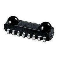
TFDU4101-TT3 Vishay, TFDU4101-TT3 Datasheet - Page 6

TFDU4101-TT3
Manufacturer Part Number
TFDU4101-TT3
Description
Infrared Transceivers SIR 115.2kbits Top View
Manufacturer
Vishay
Datasheet
1.TFDU4101-TR3.pdf
(13 pages)
Specifications of TFDU4101-TT3
Wavelength
900 nm
Continual Data Transmission
115.2 Kbit/s
Radiant Intensity
65 mW/sr
Half Intensity Angle Degrees
24 deg
Pulse Width
2.2 us
Maximum Rise Time
100 ns, 300 ns
Maximum Fall Time
100 ns, 300 ns
Operating Voltage
2.4 V to 5.5 V
Maximum Operating Temperature
+ 85 C
Minimum Operating Temperature
- 30 C
Dimensions
9.7 mm x 4.7 mm x 4 mm
Data Rate Max
115.2Kbps
Data Transmission Distance
1m
Peak Wavelength
900nm
Supply Current
90µA
Supply Voltage Range
2.4V To 5.5V
Operating Temperature Range
-30°C To +85°C
Msl
MSL 4 - 72 Hours
Data Rate
115.2kbs (SIR)
Idle Current, Typ @ 25° C
75µA
Link Range, Low Power
1m
Operating Temperature
-30°C ~ 85°C
Orientation
Top View
Shutdown
*
Size
9.7mm x 4.7mm x 4mm
Standards
IrPHY 1.0
Supply Voltage
2.4 V ~ 5.5 V
Lead Free Status / RoHS Status
Lead free / RoHS Compliant
Lead Free Status / RoHS Status
Lead free / RoHS Compliant, Lead free / RoHS Compliant
Available stocks
Company
Part Number
Manufacturer
Quantity
Price
Company:
Part Number:
TFDU4101-TT3
Manufacturer:
VISHAY
Quantity:
41 000
Part Number:
TFDU4101-TT3
Manufacturer:
VISHAY/威世
Quantity:
20 000
TFDU4101
Vishays Semiconductors
RECOMMENDED CIRCUIT DIAGRAM
Operated with a clean low impedance power supply the
TFDU4101 needs no additional external components.
However, depending on the entire system design and board
layout, additional components may be required (see figure
1). That is especially the case when separate power supplies
are used for bench tests. When using compact wiring and
regulated supplies as e. g. in phone applications in most
cases no external components are necessary.
Note
*)
The capacitor C1 is buffering the supply voltage and
eliminates the inductance of the power supply line. This one
should be a Tantalum or other fast capacitor to guarantee the
fast rise time of the IRED current. The resistor R1 is the
current limiting resistor, which may be used to reduce the
operating current to levels below the specified controlled
values for saving battery power.
Vishay's transceivers integrate a sensitive receiver and a
built-in power driver. The combination of both needs a
careful circuit board layout. The use of thin, long, resistive
and inductive wiring should be avoided.The shutdown input
Figure 2 shows an example of a typical application with a
separate supply voltage V
the IRED anode connected to the unregulated battery V
This method reduces the peak load of the regulated power
supply and saves therefore costs. Alternatively all supplies
can also be tied to only one voltage source. R1 and C1 are
not used in this case and are depending on the circuit design
in most cases not necessary.
In figure 2 an option is shown to operate the transmitter at
www.vishay.com
6
R1 is optional when reduced intensity is used.
TABLE 1 - RECOMMENDED TESTS AND APPLICATION CIRCUIT COMPONENTS
COMPONENT
C1
C2
R1
R2
V
V
GND
SD
TXD
RXD
IRED
CC
Fig. 1 - Recommended Test Circuit.
20037
C1
Depends on current to be adjusted, e. g. with V
R1
R2
irdasupportAM@vishay.com, irdasupportAP@vishay.com,
*)
S
For technical questions within your region, please contact one of the following:
and using the transceiver with
C2
RECOMMENDED VALUE
V
V
Ground
SD
TXD
RXD
IRED C
0.1 µF, ceramic
CC2
CC1
47 Ω, 0.125 W
4.7 µF, 16 V
, IRED A
Infrared Transceiver Module (SIR, 115.2 kbit/s)
batt
for IrDA
.
CC2
must be grounded for normal operation, also when the
shutdown function is not used.
The inputs (TXD, SD) and the output RXD should be directly
connected (DC - coupled) to the I/O circuit. The capacitor C2
combined with the resistor R2 is the low pass filter for
smoothing the supply voltage. R2, C1 and C2 are optional
and dependent on the quality of the supply voltages V
and injected noise. An unstable power supply with dropping
voltage during transmission may reduce the sensitivity (and
transmission range) of the transceiver.
The placement of these parts is critical. It is strongly
recommended to position C2 as close as possible to the
transceiver power supply pins.
When extended wiring is used (bench tests!) the inductance
of the power supply can cause dynamically a voltage drop at
V
fast current rise time. In that case another 4.7 µF (type, see
table under C1) at V
Under
RF-transmitter antenna on top of the transceiver, we
recommend to protect all inputs by a low-pass filter, as a
minimum a 12 pF capacitor, especially at the RXD port. The
transceiver itself withstands EMI at GSM frequencies above
500 V/m. When interference is observed, the wiring to the
inputs picks it up. It is verified by DPI measurements that as
long as the interfering RF - voltage is below the logic
threshold levels of the inputs and equivalent levels at the
outputs no interferences are expected.
One should keep in mind that basic RF - design rules for
circuit design should be taken into account. Especially longer
signal lines should not be used without termination. See e.g.
"The Art of Electronics" Paul Horowitz, Winfield Hill, 1989,
Cambridge University Press, ISBN: 0521370957.
two different power levels to switch for long range to low
power mode for e.g. saving power for IrDA application but
use the full range specification for remote control. The
additional components are marked in the figure.
For operating at RS232 ports TOIM4232 is recommended as
ENDEC.
®
CC2
= 3.3 V 56 Ω is an option for minimum low power operation
Applications
. Often some power supplies are not able to follow the
extreme
irdasupportEU@vishay.com
CC2
EMI
CRCW-1206-47R0-F-RT1
VISHAY PART NUMBER
VJ 1206 Y 104 J XXMT
will be helpful.
293D 475X9 016B
conditions
Document Number: 81288
as
Rev. 1.5, 08-Jul-09
placing
CC1
an


