P222-155.52M Connor-Winfield, P222-155.52M Datasheet - Page 2
P222-155.52M
Manufacturer Part Number
P222-155.52M
Description
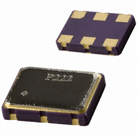
OSC 155.5200MHZ 2.5V LVPECL SMD
Manufacturer
Connor-Winfield
Series
Pr
Type
Standardr
Datasheet
1.P123-155.52M.pdf
(2 pages)
Specifications of P222-155.52M
Supply Voltage
2.5V
Frequency
155.52MHz
Frequency Stability
±50ppm
Operating Temperature
-40°C ~ 85°C
Current - Supply (max)
90mA
Mounting Type
Surface Mount
Size / Dimension
0.276" L x 0.197" W (7.00mm x 5.00mm)
Height
0.059" (1.50mm)
Package / Case
SMD 7.00mm x 5.00mm
Supply Current
90mA
Lead Free Status / RoHS Status
Lead free / RoHS Compliant
Other names
CW616
P222 155.52M
P222155.52M
P222 155.52M
P222155.52M
Available stocks
Company
Part Number
Manufacturer
Quantity
Price
Company:

Part Number:
P222-155.52M
Manufacturer:
Connor-Winfield
Quantity:
135


Notes:
1. Includes calibration @ 25°C, frequency stability vs. change in temperature, supply voltage and load variations, shock
and vibration and 20 years aging. Models P242, P243 P244 and P245 are not available above 260 MHz.
2. Models P242, P243 P244 and P245 are not available above 260 MHz.
3. When the oscillator is disabled the outputs are at high impedance. Outputs are enabled with no connection on E/D pad.
4. Outputs must be terminated into 50 ohms to Vcc – 2V or Thevenin equivalent.
5. Duty cycle measured at 50% of output voltage swing.
Type
LVPECL
Clock Series
5x7 mm
Package
Vibration:
Shock:
Soldering Process; RoHS compliant lead free. See soldering profile on page 2.
Attention: Models P242, P243, P244 and P245 are not available above 260 MHz.
P
Vcc = Vcc2
0 to 70, +/-20ppm, 3.3Vdc, E/D Pad 1, Output Frequency 155.52MHz
Mechanical Shock per Mil Std 883E Method 2002.4 Test Condition B.
1 = 0 to 70°C
2 = -40 to 85°C
3 = 0 to 85°C
4 = -20 to 70°C
Hermetically sealed ceramic package and metal cover
Specifications subject to change without notice. All dimensions in inches. © Copyright 2010 The Connor-Winfield Corporation
Temperature
Function:
Low:
High or Open: Enabled
2.5V
3.3V
Vcc
Range
Vibration per Mil Std 883E Method 2007.3 Test Condition A.
Environmental Characteristics
1
250 Ohms
130 Ohms
Tape and Reel Dimensions
R1 / R3
Enable / Disable Function
Package Characteristics
Ordering Information
P123-155.52M = LVPECL Output,
Enable /
Disable
4 = ±20 ppm
1 = ±25 ppm
2 = ±50 ppm
3 = ±100 ppm
62.5Ohms
N/C
82 Ohms
Example: Part Number
or
R2 /R4
Frequency
Output
Disabled (High Impedance)
Test Circuit
Stability
2
6 5 4
1 2 3
2 = 2.5 Vdc, E/D Pad 1
3 = 3.3 Vdc, E/D Pad 1
4 = 3.3 Vdc, E/D Pad 2
5 = 2.5 Vdc, E/D Pad 2
Supply Voltage
R2
R1
3
R3
R4
Dimensional Tolerance: ±.02” (.508mm)
Output Frequency
Frequency Format
-xxx.xM Min
-xxx.xxxxxxM Max
*Amount of numbers
after the decimal
point. M = MHz
- 155.52M
±.005” (.127mm)
1:
2
3:
4:
5:
6:
Models: Pxx2, Pxx3
Enable / Disable
N/C
Ground
Output Q
Complementary Output Q
Supply Voltage (Vcc)
(5.0mm)
Duty Cycle
50%
20%
0.197
(1.50mm)
80%
.059
Q
Q
tr
CW 0946
Temperature
Suggested Pad Layout
155.52M
(4.2mm)
(7.0mm)
260°C
220°C
180°C
150°C
120°C
0
0.165
0.275
P123
Pad Connections
Output Waveform
Package Outline
Solder Profile
View
Top
6
1
120 S
Max.
(5.08mm)
0.200
5
1:
2
3:
4:
5:
6:
2
(2.6mm)
0.102
Models Pxx4, Pxx5
Bulletin
Page
Revision
Date
360 Sec. Max.
2111 Comprehensive Drive
N/C
Enable / Disable
Ground
Output Q
Complementary Output Q
Supply Voltage (Vcc)
60 S
Max.
tf
10 S
260°C
4
3
Aurora, Illinois 60505
Phone: 630- 851- 4722
(2.54mm)
www.conwin.com
Fax: 630- 851- 5040
0.100
(2.0mm)
(1.78mm)
0.079
Dimensional Tolerance
0.070
Ground
+/-0.008 (+/-0.2mm)
Capacitor
Bypass
0.01uF
Time
22 MAr 2010
(1.4mm)
0.055
EC217
2 of 2
10
Related parts for P222-155.52M
Image
Part Number
Description
Manufacturer
Datasheet
Request
R

Part Number:
Description:
OSC 125.0000MHZ 2.5V LVPECL SMD
Manufacturer:
Connor-Winfield
Datasheet:
Part Number:
Description:
OSC 100.0000MHZ 2.5V LVPECL SMD
Manufacturer:
Connor-Winfield
Datasheet:
Part Number:
Description:
OSC 156.2500MHZ 2.5V LVPECL SMD
Manufacturer:
Connor-Winfield
Datasheet:

Part Number:
Description:
CABLE EXTENSION PS/2 M-F 6'
Manufacturer:
Tripp Lite
Datasheet:

Part Number:
Description:
CABLE EXTENSION PS/2 M-F 10'
Manufacturer:
Tripp Lite
Datasheet:

Part Number:
Description:
PS/2 Keyboard/Mouse Extension Cable MinDIN6M/F - 25
Manufacturer:
Tripp Lite
Part Number:
Description:
PS/2 Keyboard/Mouse Extension Cable MinDIN6M/F - 50
Manufacturer:
Tripp Lite

Part Number:
Description:
OSC 10.0000MHZ 3.3V +-50PPM SMD
Manufacturer:
Connor-Winfield

Part Number:
Description:
HCMOS SM CLOCK WITH ENABLE/DISABLE
Manufacturer:
CONNOR-WINFIELD [Connor-Winfield Corporation]
Datasheet:
Part Number:
Description:
3.3V SURFACE MOUNT HCMOS CLOCK OSCILLATOR
Manufacturer:
CONNOR-WINFIELD [Connor-Winfield Corporation]
Datasheet:
Part Number:
Description:
3.3V SURFACE MOUNT HCMOS CLOCK OSCILLATOR
Manufacturer:
CONNOR-WINFIELD [Connor-Winfield Corporation]
Datasheet:
Part Number:
Description:
HCMOS SM CLOCK WITH ENABLE/DISABLE
Manufacturer:
CONNOR-WINFIELD [Connor-Winfield Corporation]
Datasheet:
Part Number:
Description:
SURFACE MOUNT J LEADED HCMOS CLOCK OSCILLATOR
Manufacturer:
CONNOR-WINFIELD [Connor-Winfield Corporation]
Datasheet: