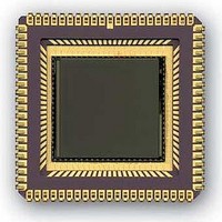
CYIS1SM1000-EVAL Cypress Semiconductor Corp, CYIS1SM1000-EVAL Datasheet - Page 15

CYIS1SM1000-EVAL
Manufacturer Part Number
CYIS1SM1000-EVAL
Description
MCU, MPU & DSP Development Tools 1M Pixel Radiation Hard CMOS Img Snsr
Manufacturer
Cypress Semiconductor Corp
Datasheet
1.CYIS1SM1000-EVAL.pdf
(24 pages)
Specifications of CYIS1SM1000-EVAL
Lead Free Status / RoHS Status
Lead free / RoHS Compliant
Cypress Semiconductor Corporation 3901 North First Street
Contact:
Pin
10
11
12
13
14
15
16
17
18
19
20
21
22
23
24
25
26
27
1
2
3
4
5
6
7
8
9
STAR-1000
Datasheet
Pin name
A3
A4
A5
A6
A7
A8
A9
LD_Y
LD_X
VDDA
GNDD
GNDA
CLK_X
RESET_DS
VDDD
RESET
S
R
NBIAS_DEC
A_IN2
A_IN3
A_IN1
A_SEL1
A_SEL0
NBIAS_OAMP
PBIAS
G1
info@Fillfactory.com
Table 7: Pin list of the STAR-1000 sensor
Pin type
Input
Input
Input
Input
Input
Input
Input
Input
Input
Supply
Ground
Ground
Input
Input
Supply
Input
Input
Input
Input
Input
Input
Input
Input
Input
Input
Input
Input
Document #:38-05714 Rev.**(Revision 6.5)
Pin description
Digital input.
Address inputs for row and column addressing.
A9=LSB, A0=MSB.
Digital Input. Latch address (A0…A9) to Y-register (0 =
track, 1 = hold).
Digital Input. Latch address (A0…A9) to X-register (0 =
track, 1 = hold).
Analog power supply of the imager (typical 5V).
Digital ground of the imager.
Analog ground of the imager.
Digital input. Clock X-register (output valid & stable
when CLK_X is high).
Digital input (high active). Resets row indicated by Y-
address (see sensor timing diagram).
RESET_DS can be used for dual-slope integration (see
FAQ).
Connect to GND for normal operation.
Digital supply of the image sensor.
Digital input (high active). Resets row indicated by Y-
address (see sensor timing diagram).
Digital input (high active). Control signal for column
amplifier (see sensor timing diagram).
Digital input (high active). Control signal for column
amplifier (see sensor timing diagram).
Analog input. Biasing of address decoder.
Connect with 100kΩ to VDDA and decouple with 100
nF to GND.
Additional analog inputs. For proper conversion with
on-chip ADC the input signal must lie within the output
signal range of the image sensor (approximately +2V to
+4V).
Selection of analog channel: ‘00’ selects image sensor
(’01’ selects A_IN1; ‘10’ A_IN2 and ‘11’ A_IN3).
Analog input. Bias of output amplifier (speed/power
control).
Connect with 100kΩ to VDDA and decouple with 100
nF to GND for 12.5 MHz output rate (lower resistor
values yield higher maximal pixel rates at the cost of
extra power dissipation).
Analog input. Biasing of the multiplexer circuitry.
Connect with 20kΩ to GND and decouple with 100nF to
VDD.
Digital input. Select output amplifier gain value: G0 =
San Jose, CA 95134 408-943-2600
Page 15 of 24


