LG1152 DAISY CHAIN Actel, LG1152 DAISY CHAIN Datasheet
LG1152 DAISY CHAIN
Specifications of LG1152 DAISY CHAIN


Related parts for LG1152 DAISY CHAIN

LG1152 DAISY CHAIN Summary of contents
Page 1
... This creates a greater standoff, providing a flexible interconnection with improved thermal characteristic, significantly increasing the thermal fatigue life of the package solder joint. Actel has selected the CCGA technology as part of its high-density, high I/O count hermetic package offering. A 624-pin CCGA (CG624), 1152 pin-CCGA (CG1152), and 1272-pin CCGA (CG1272) are offered for ...
Page 2
... Figure 3 • CG1272 Package Top and Bottom View CCGA Package Description The CCGA is a multi-layer ceramic package with attributes including: 1. Dark ceramic, same material as Actel's CQ208, CQ256, and CQ352 packages 2. The solder column is either 90Pb/10Sn or 80Pb/20Sn, with a copper ribbon (refer to Figure 5 on page 3) attached to the ceramic substrate I/O pads via eutectic 37/63 Pb/Sn, forming a eutectic solder joint ...
Page 3
Figure 4 • 90Pb/10Sn Column Side View and Tip View, with 20 mils Diameter Figure 5 • Change to 80Pb/20Sn Column Side View and Tip View, with 20 mils Diameter 90Pb/10Sn Column or 80Pb/20Sn with Cu Ribbon Column Figure 6 ...
Page 4
... Six Sigma. Six Sigma's CCGA qualification summary may be obtained by contacting either Actel or Six Sigma directly. In addition to the qualification data provided by BAE Systems and Six Sigma, Actel completed its own CCGA board-level thermal cycling test on both the 90Pb/10Sn column and 80Pb/20Sn column devices. This ...
Page 5
... Manufacturing Handling and Assembly Handling CCGA Packages During Manufacturing and Programming Due to the difficulty in handling the solder columns, Actel initially processes the CCGA packages in the Land Grid Array (LGA) format (column pins are not attached at this stage; see and Figure 9 on page 6) ...
Page 6
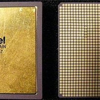
... Figure 9 • LG1272 Top and Bottom View Handling of CCGA Packaged Parts 1. Actel ships each CCGA packaged part in a tray carrier with a column protection feature. The tray carrier is then stored in a black ESD-protective jewel box and sealed in a dry pack. See page 7 ...
Page 7
Figure 10 • From Top to Bottom: CG624, CG1152, and CG1272 in their Respective Tray Carriers Ceramic Column Grid Array 7 ...
Page 8
... End users may require incoming visual inspection of CCGA devices after they are received from Actel. Precaution must be exercised to not only ensure the CCGA devices are not damaged during inspection but also make sure devices are seated properly on the tray carrier, which is stored in the black jewel box and secured there with extra ESD tape ...
Page 9
... No cracks are permitted within the solder column body greater than 3 mils in length. – No loose non-conductive fibers are acceptable, regardless of size, during final inspection. Operators can remove loose fibers with a 20 psi air gun as needed. Actel recommends, however, that end customers inspect and air blow parts prior to attaching CCGA packages to their boards. ...
Page 10
Ceramic Column Grid Array Appendix – CCGA Package Dimensioning and Assembly Parameters (reference only) CGGA Package Outline Drawings 32.50 ± 0.33 (1.50 × 45°) A CHAMFER INDEX MARK (Ø1.80) (0.50 × 45°) CHAMFER Notes: 1. Solder Column Material: 90Pb/10Sn or ...
Page 11
D CHAMFER 3X (0.50 × 45°) CHAMFER SYMBOL DIMENSION RTAX2000S D 30.734 ± 0.076 E 30.734 ± 0.076 Notes: 1. Solder Column Material: 80Pb/20Sn with Cu Ribbon 2. Units: mm Figure 12 • Outline ...
Page 12
Ceramic Column Grid Array 37.500 ± 0.380 D (1.50 × 45°) CHAMFER 3X (0.50 × 45°) CHAMFER SYMBOL DIMENSION RTAX4000S DAISY CHAIN D 34.036 ± 0.076 34.036 ± 0.076 E 34.036 ± 0.076 34.036 ± 0.076 Notes: 1. Solder Column ...
Page 13
PCB Pad Layout Reference Solder Mask Window (diameter A) Mounting Pad 2 (diameter B) Via Solder Mask Window (diameter D) Via (diameter E) Land G Typical (diameter F) All dimensions are in mm unless otherwise specified. Notes: 1. Functional surface ...
Page 14
Ceramic Column Grid Array Figure 15 • Solder Paste on CCGA624 PCB (upper) and on CCGA1152/1272 (lower ...
Page 15
PCB Reflow Reference Notes: 1. Probe 1 is mounted on PCB top surface and in center of package. 2. Probe 2 is mounted on top LID of package. 3. Probe 3 is mounted on PCB top surface. 4. Adjust reflow ...
Page 16
... Ceramic Column Grid Array Related Documents Thermal Cycling Test Report for Ceramic Column Grid Array Packages--CCGA http://www.actel.com/documents/CCGA_board_level_testing_report.pdf Ceramic Column Grid Array Assembly and Rework http://www-01.ibm.com/chips/techlib/techlib.nsf/techdocs/630AFA7BD7DE3FED87256C0100558D50 List of Changes The following table lists critical changes that were made in the current version of the chapter. ...
Page 17
... Actel and the Actel logo are registered trademarks of Actel Corporation. All other trademarks are the property of their owners. Actel Corporation Actel Europe Ltd. 2061 Stierlin Court River Court, Meadows Business Park Mountain View, CA Station Approach, Blackwater 94043-4655 Camberley Surrey GU17 9AB ...