DR7003-EV RFM, DR7003-EV Datasheet - Page 4
DR7003-EV
Manufacturer Part Number
DR7003-EV
Description
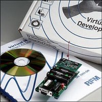
RF Modules & Development Tools 3G Transceiver Eval Module 303.825 MHz
Manufacturer
RFM
Datasheet
1.DR7003-DK.pdf
(7 pages)
Specifications of DR7003-EV
Lead Free Status / RoHS Status
Lead free / RoHS Compliant


www.RFM.com
©2008 by RF Monolithics, Inc.
Pin
10
12
13
14
15
16
17
18
11
9
19.2KBPS
OOK/ASK
4.8KBPS/
Not Used
Not Used
RXDCLK
CFGDAT
CFGCLK
3G SEL
SLEEP
Name
E-mail: info@rfm.com
SVEN
In/Out
In/Out
In/Out
Out
In
In
In
In
In
Logic Input (CMOS compatible). This pin, in 3G mode, selects the operation of the TR7003. Pull this pin
‘High’ for OOK Transmit/Receive mode. Pull this pin ‘Low’ for ASK Transmit/Receive mode. Do not allow this
pin to float.
Logic Input (CMOS compatible). This pin, in 3G mode, puts the TR7003 into Sleep mode. Pull this pin ‘High’
for Sleep Mode. Pull this pin ‘Low’ for operation mode. Do not allow this pin to float.
Logic Input (CMOS compatible). This pin, in 3G mode, enables the Start Vector Recognition circuit. The
TR7003 will not output a recovered clock on RXDCLK (pin 16) until the start vector, 0xE2E2, has been recog-
nized. Pull this pin ‘High’ to enable Start Vector Recognition. Pull this pin ‘Low’ then ‘High’ to reset the Start
Vector Recognition circuit. Do not allow this pin to float.
Keep this pin pulled ‘Low’.
Keep this pin pulled ‘Low’.
Logic Input (CMOS compatible). This pin, in 3G mode, selects the receive data rate of the DR7003. Pull this
pin ‘High’ to select 4.8kbps. Pull this pin ‘Low’ to select 19.2kbps. Do not allow this pin to float.
NOTE: Operating at 19.2kbps will require the value of C4, C5 and R4 to change to accommodate the
higher data rate. See the TR7003 datasheet for recommended component values.
Logic Input (CMOS compatible). This pin sets the processor to operate in 3G mode. The power-up operating
configuration of the TR7003 device is controlled by the J2 jumper setting. When DC power is applied to the
DR7003 with J2 installed across 2-3, this pin should be pulled ‘High’ immediately after power-up to initiate 3G
mode. Failure to pull pin 15 ‘High’ after power-up will cause the processor to remain inactive. Pulling this pin
‘High’ wakes the processor for 3G mode operation. When DC power is applied to the DR7003 with J2 installed
across 1-2, this pin should be held ‘Low’ to operate in 2G mode. Do not allow this pin to float.
RXDCLK is the clock output from the data and clock recovery circuit. RXDCLK is a CMOS output. When the
radio’s internal data and clock recovery circuit is not used, RXDCLK is a steady low value. When the internal
data and clock recovery is used, RXDCLK is low until a packet start symbol is detected at the output of the
data slicer. Each bit following the start symbol is output at RXDATA on the rising edge of a RXDCLK pulse,
and is stable for reading on the falling edge of the RXDCLK pulse. Once RXDCLK is activated by the detec-
tion of a start symbol, it remains active until SVEN (pin 11) is reset. See Pin 11 description.
In 3G control mode, CFGDAT is a bi-directional CMOS logic pin. When CFG (Pin 19) is set to a logic 1, con-
figuration data can be clocked into or out of the radio’s configuration registers through CFGDAT using CFG-
CLK (Pin 18). Data clocked into CFGDAT is transferred to a control register each time a group of 8 bits is
received. Pulses on CFGCLK are used to clock configuration data into and out of the radio through CFGDAT.
When writing through CFGDAT, a data bit is clocked into the radio on the rising edge of a CFGCLK pulse.
When reading through CFGDAT, data is output on the rising edge of the CFGCLK pulse and is stable for
reading on the falling edge of the CFGCLK. Refer to the TR7003 datasheet for detailed timing. This pin is a
high impedance input (CMOS compatible) in 2G mode. This pin must be held at a logic level. Do not allow
this pin to float.
In 3G control mode, pulses on CFGCLK are used to clock configuration data into and out of the radio through
CFGDAT (Pin 17). When writing to CFGDAT, a data bit is clocked into the radio on the rising edge of a CFG-
CLK pulse. When reading through CFGDAT, data is stable for reading on the falling edge of the CFGCLK.
Refer to the TR7003 datasheet for detailed timing. This pin is a high impedance input (CMOS compatible) in
2G mode. Do not allow this pin to float.
Description
DR7003 - 4/8/08
Page 4 of 7
Related parts for DR7003-EV
Image
Part Number
Description
Manufacturer
Datasheet
Request
R

Part Number:
Description:
3G DEVELOPMENT KIT 303.825 MHZ
Manufacturer:
RFM
Datasheet:

Part Number:
Description:
RF Transceiver 3G Transceiver Module 303.825 MHz
Manufacturer:
RFM
Datasheet:

Part Number:
Description:
ASH RX 115.2 KBPS 433.92 MHZ
Manufacturer:
RFM
Datasheet:

Part Number:
Description:
RFIC TRANCEIVER MULTI-CHANNEL FS
Manufacturer:
RFM
Datasheet:

Part Number:
Description:
ASH TX 115.2 KBPS 433.92 MHZ
Manufacturer:
RFM
Datasheet:
Part Number:
Description:
Filters 1602MHz BW=61MHz
Manufacturer:
RFM
Datasheet:

Part Number:
Description:
RESONATOR, SM3030-6
Manufacturer:
RFM
Datasheet:

Part Number:
Description:
RESONATOR, SM3030-6
Manufacturer:
RFM
Datasheet:

Part Number:
Description:
RESONATOR, SM3030-6
Manufacturer:
RFM
Datasheet:

Part Number:
Description:
RESONATOR, SM5035-4
Manufacturer:
RFM
Datasheet:

Part Number:
Description:
10-Terminal Ceramic Surface-Mount Case 7 x 5 mm Nominal Footprint
Manufacturer:
RFM [RF Monolithics, Inc]
Datasheet:
Part Number:
Description:
QUAD-BAND GSM850/GSM/DCS/PCS POWER AMP MODULE
Manufacturer:
RFM [RF Monolithics, Inc]
Datasheet:
Part Number:
Description:
402 to 405 MHz Medical Band Front-end Filter
Manufacturer:
RFM [RF Monolithics, Inc]
Datasheet:
Part Number:
Description:
674.03 MHz SAW Resonator
Manufacturer:
RFM [RF Monolithics, Inc]
Datasheet: