NSBC114EDXV6T5 ON Semiconductor, NSBC114EDXV6T5 Datasheet
NSBC114EDXV6T5
Specifications of NSBC114EDXV6T5
Available stocks


Related parts for NSBC114EDXV6T5

NSBC114EDXV6T5 Summary of contents
Page 1
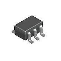
... NSBC114EDXV6T1, NSBC114EDXV6T5 Preferred Devices Dual Bias Resistor Transistors NPN Silicon Surface Mount Transistors with Monolithic Bias Resistor Network The BRT (Bias Resistor Transistor) contains a single transistor with a monolithic bias network consisting of two resistors; a series base resistor and a base−emitter resistor. These digital transistors are designed to replace a single device and its external resistor bias network ...
Page 2
... NSBC114EDXV6T1, NSBC114EDXV6T5 DEVICE MARKING, ORDERING, AND RESISTOR VALUES Device† NSBC114EDXV6T1 NSBC124EDXV6T1 NSBC144EDXV6T1 NSBC114YDXV6T1 NSBC114TDXV6T1 (Note 2) NSBC143TDXV6T1 (Notes 2) NSBC113EDXV6T1 (Note 2) NSBC123EDXV6T1 (Notes 2) NSBC143EDXV6T1 (Notes 2) NSBC143ZDXV6T1 (Notes 2) NSBC124XDXV6T1 (Notes 2) NSBC123JDXV6T1 (Note 2) NSBC115EDXV6T1 (Notes 2) NSBC144WDXV6T1 (Notes 2) †The “G’’ suffix indicates Pb−Free package available. ...
Page 3
... NSBC114EDXV6T1, NSBC114EDXV6T5 ELECTRICAL CHARACTERISTICS Characteristic ON CHARACTERISTICS (Note 4) DC Current Gain ( 5.0 mA Collector-Emitter Saturation Voltage ( mA 0 NSBC143EDXV6T1/NSBC143ZDXV6T1/NSBC124XDXV6T1 Output Voltage ( 1 1 1 1.0 kW Output Voltage (off 5 0 1 0.050 1 1.0 kW Input Resistor Resistor Ratio NSBC113EDXV6T1/NSBC123EDXV6T1/NSBC143EDXV6T1 4. Pulse Test: Pulse Width < ...
Page 4
... NSBC114EDXV6T1, NSBC114EDXV6T5 300 250 200 150 100 R = 833°C/W 50 qJA 0 − AMBIENT TEMPERATURE (°C) A Figure 1. Derating Curve http://onsemi.com 4 100 150 ...
Page 5
... NSBC114EDXV6T1, NSBC114EDXV6T5 TYPICAL ELECTRICAL CHARACTERISTICS — NSBC114EDXV6T1 0.1 0.01 0.001 COLLECTOR CURRENT (mA) C Figure 2. V versus I CE(sat REVERSE BIAS VOLTAGE (VOLTS) R Figure 4. Output Capacitance 0 0.1 0 Figure 6. Input Voltage versus Output Current 1000 T = −25°C A 25°C 75°C 100 100 75° MHz ...
Page 6
... NSBC114EDXV6T1, NSBC114EDXV6T5 TYPICAL ELECTRICAL CHARACTERISTICS — NSBC124EDXV6T1 −25°C A 0.1 0.01 0.001 COLLECTOR CURRENT (mA) C Figure 7. V versus I CE(sat REVERSE BIAS VOLTAGE (VOLTS) R Figure 9. Output Capacitance 100 0.1 0 Figure 11. Input Voltage versus Output Current 1000 25°C 75°C 100 100 MHz ...
Page 7
... NSBC114EDXV6T1, NSBC114EDXV6T5 TYPICAL ELECTRICAL CHARACTERISTICS — NSBC144EDXV6T1 −25°C A 0.1 0. COLLECTOR CURRENT (mA) C Figure 12. V versus I CE(sat) 1 0.8 0.6 0.4 0 REVERSE BIAS VOLTAGE (VOLTS) R Figure 14. Output Capacitance 100 0.1 0 Figure 16. Input Voltage versus Output Current 1000 25°C 100 75° 100 MHz ...
Page 8
... NSBC114EDXV6T1, NSBC114EDXV6T5 TYPICAL ELECTRICAL CHARACTERISTICS — NSBC114YDXV6T1 0.1 0.01 0.001 COLLECTOR CURRENT (mA) C Figure 17. V versus I CE(sat) 4 3.5 3 2.5 2 1 REVERSE BIAS VOLTAGE (VOLTS) R Figure 19. Output Capacitance 0.1 0 Figure 21. Input Voltage versus Output Current 300 −25°C 250 A 25°C 200 75° ...
Page 9
... NSBC114EDXV6T1, NSBC114EDXV6T5 D −X− −Y− 0.08 (0.003) M *For additional information on our Pb−Free strategy and soldering details, please download the ON Semiconductor Soldering and Mounting Techniques Reference Manual, SOLDERRM/D. ON Semiconductor and are registered trademarks of Semiconductor Components Industries, LLC (SCILLC). SCILLC reserves the right to make changes without further notice to any products herein ...