1N5921BG ON Semiconductor, 1N5921BG Datasheet
1N5921BG
Specifications of 1N5921BG
1N5921BGOS
Available stocks


Related parts for 1N5921BG

1N5921BG Summary of contents
Page 1
... If these limits are exceeded, device functional operation is not implied, damage may occur and reliability may be affected. *For additional information on our Pb−Free strategy and soldering details, please download the ON Semiconductor Soldering and Mounting Techniques Reference Manual, SOLDERRM/D. © Semiconductor Components Industries, LLC, 2006 Symbol ...
Page 2
ELECTRICAL CHARACTERISTICS (T = 30°C unless otherwise noted 1.5 V Max @ I = 200 mAdc for all types Symbol Parameter V Reverse Zener Voltage @ Reverse Current ZT Z Maximum ...
Page 3
... G 1N5956B 190 Devices listed in bold, italic are ON Semiconductor Preferred devices. Preferred devices are recommended choices for future use and best overall value. †The “G’’ suffix indicates Pb−Free package available. 1. TOLERANCE AND TYPE NUMBER DESIGNATION Tolerance designation − device tolerance of ±5% are indicated by a “B” suffix. ...
Page 4
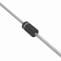
Series PACKAGE DIMENSIONS AXIAL LEAD CASE 59−10 ISSUE POLARITY INDICATOR OPTIONAL AS NEEDED F (SEE STYLES) K NOTES: 1. DIMENSIONING AND TOLERANCING PER ANSI Y14.5M, 1982. 2. CONTROLLING DIMENSION: INCH. 3. ALL RULES ...