MMSZ27T1G ON Semiconductor, MMSZ27T1G Datasheet

DIODE ZENER 27V 500MW SOD-123

MMSZ27T1G

Manufacturer Part Number
MMSZ27T1G
Description
DIODE ZENER 27V 500MW SOD-123
Manufacturer
ON Semiconductor
Datasheet

Specifications of MMSZ27T1G

Voltage - Zener (nom) (vz)
27V
Voltage - Forward (vf) (max) @ If
900mV @ 10mA
Current - Reverse Leakage @ Vr
50nA @ 18.9V
Tolerance
±5%
Power - Max
500mW
Impedance (max) (zzt)
80 Ohm
Mounting Type
Surface Mount
Package / Case
SOD-123
Operating Temperature
-55°C ~ 150°C
Zener Voltage
27 V
Voltage Tolerance
5 %
Zener Current
10 mA
Power Dissipation
500 mW
Maximum Reverse Leakage Current
0.05 uA
Maximum Zener Impedance
80 Ohms
Maximum Operating Temperature
+ 150 C
Mounting Style
SMD/SMT
Minimum Operating Temperature
- 55 C
Lead Free Status / RoHS Status
Lead free / RoHS Compliant
Other names
MMSZ27T1G
MMSZ27T1GOSTR

Available stocks

Company
Part Number
Manufacturer
Quantity
Price
Part Number:
MMSZ27T1G
Manufacturer:
ON
Quantity:
3 000
Part Number:
MMSZ27T1G
Manufacturer:
ON Semiconductor
Quantity:
18 000
Part Number:
MMSZ27T1G
Manufacturer:
ON
Quantity:
30 000
Part Number:
MMSZ27T1G
Manufacturer:
ON
Quantity:
5 216
MMSZ2V4T1 Series
Zener Voltage Regulators
500 mW SOD−123 Surface Mount
surface mount plastic SOD−123 package. These devices provide a
convenient alternative to the leadless 34−package style.
Features
Mechanical Characteristics
CASE:
FINISH:
MAXIMUM CASE TEMPERATURE FOR SOLDERING PURPOSES:
POLARITY:
FLAMMABILITY RATING:
Maximum ratings are those values beyond which device damage can occur.
Maximum ratings applied to the device are individual stress limit values (not
normal operating conditions) and are not valid simultaneously. If these limits are
exceeded, device functional operation is not implied, damage may occur and
reliability may be affected.
1. FR−5 = 3.5 X 1.5 inches.
2. Thermal Resistance measurement obtained via infrared Scan Method.
MAXIMUM RATINGS
© Semiconductor Components Industries, LLC, 2006
Juanuary, 2006 − Rev. 9
Total Power Dissipation on FR−5 Board,
(Note 1) @ T
Derated above 75°C
Thermal Resistance, Junction−to−Ambient
(Note 2)
Thermal Resistance, Junction−to−Lead
(Note 2)
Junction and Storage Temperature Range
Three complete series of Zener diodes are offered in the convenient,
260°C for 10 Seconds
500 mW Rating on FR−4 or FR−5 Board
Wide Zener Reverse Voltage Range − 2.4 V to 56 V
Package Designed for Optimal Automated Board Assembly
Small Package Size for High Density Applications
ESD Rating of Class 3 (>16 kV) per Human Body Model
Pb−Free Packages are Available
Void-free, transfer-molded, thermosetting plastic case
Corrosion resistant finish, easily Solderable
Cathode indicated by polarity band
L
= 75°C
Rating
UL 94 V−0
Symbol
T
R
R
J
P
, T
qJA
qJL
D
stg
−55 to +150
Max
500
340
150
6.7
1
mW/°C
°C/W
°C/W
Unit
mW
°C
†For information on tape and reel specifications,
See specific marking information in the device marking
column of the Electrical Characteristics table on page 3 of
this data sheet.
MMSZxxxT1
MMSZxxxT3
including part orientation and tape sizes, please
refer to our Tape and Reel Packaging Specifications
Brochure, BRD8011/D.
Device
(Note: Microdot may be in either location)
DEVICE MARKING INFORMATION
ORDERING INFORMATION
Cathode
xx
M
G
MARKING DIAGRAM
1
http://onsemi.com
1
1
= Device Code
= Date Code
= Pb−Free Package
(Pb−Free)
(Pb−Free)
SOD−123
SOD−123
Package
CASE 425
SOD−123
STYLE 1
Publication Order Number:
xx M G
G
10,000/Tape & Reel
3000/Tape & Reel
Anode
2
2
MMSZ2V4T1/D
Shipping

Related parts for MMSZ27T1G

MMSZ27T1G Summary of contents

Page 1

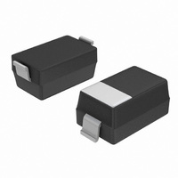
MMSZ2V4T1 Series Zener Voltage Regulators 500 mW SOD−123 Surface Mount Three complete series of Zener diodes are offered in the convenient, surface mount plastic SOD−123 package. These devices provide a convenient alternative to the leadless 34−package style. Features • 500 ...

Page 2

ELECTRICAL CHARACTERISTICS otherwise noted 0.95 V Max mA Symbol Parameter V Reverse Zener Voltage @ Reverse Current ZT Z Maximum Zener Impedance @ Reverse Leakage ...

Page 3

ELECTRICAL CHARACTERISTICS Device † Min Marking Device MMSZ2V4T1 T1 2.28 MMSZ2V7T1 T2 2.57 MMSZ3V0T1* T3 2.85 MMSZ3V3T1 T4 3.14 MMSZ3V6T1 T5 3.42 MMSZ3V9T1 U1 3.71 MMSZ4V3T1 U2 4.09 MMSZ4V7T1 U3 4.47 MMSZ5V1T1 U4 4.85 MMSZ5V6T1* U5 5.32 MMSZ6V2T1* V1 5.89 ...

Page 4

ELECTRICAL CHARACTERISTICS Device † Min Marking Device MMSZ27T1 Y1 25.65 MMSZ30T1* Y2 28.50 MMSZ33T1 Y3 31.35 MMSZ36T1* Y4 34.20 MMSZ39T1* Y5 37.05 MMSZ43T1* Z1 40.85 MMSZ47T1 Z2 44.65 MMSZ51T1* Z3 48.45 MMSZ56T1 Z4 53.20 6. The type numbers shown have ...

Page 5

TYPICAL T VALUES C FOR MMSZ2V4T1 SERIES −1 − 2 − NOMINAL ZENER VOLTAGE (V) Z Figure 1. Temperature Coefficients (Temperature ...

Page 6

V BIAS 1 V BIAS 100 BIAS AT 50 NOM NOMINAL ZENER VOLTAGE (V) Z Figure 7. Typical Capacitance 100 10 1 0.1 0. ...

Page 7

... *For additional information on our Pb−Free strategy and soldering details, please download the ON Semiconductor Soldering and Mounting Techniques Reference Manual, SOLDERRM/D. ON Semiconductor and are registered trademarks of Semiconductor Components Industries, LLC (SCILLC). SCILLC reserves the right to make changes without further notice to any products herein. SCILLC makes no warranty, representation or guarantee regarding the suitability of its products for any particular purpose, nor does SCILLC assume any liability arising out of the application or use of any product or circuit, and specifically disclaims any and all liability, including without limitation special, consequential or incidental damages. “ ...

Related keywords