NCP512SQ25T2G ON Semiconductor, NCP512SQ25T2G Datasheet
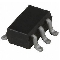
IC REG VOLTAGE 180MA 2.5V SC88A

NCP512SQ25T2G

Manufacturer Part Number
NCP512SQ25T2G
Description
IC REG VOLTAGE 180MA 2.5V SC88A
Manufacturer
ON Semiconductor
Datasheet

Specifications of NCP512SQ25T2G

Regulator Topology
Positive Fixed
Voltage - Output
2.5V
Voltage - Input
Up to 6V
Voltage - Dropout (typical)
0.22V @ 80mA
Number Of Regulators
1
Current - Output
200mA
Current - Limit (min)
-
Operating Temperature
-40°C ~ 85°C
Mounting Type
Surface Mount
Package / Case
6-TSSOP (5 lead), SC-88A, SOT-353
Number Of Outputs
1
Input Voltage Max
6 V
Output Voltage
2.5 V
Output Type
Fixed
Dropout Voltage (max)
300 mV
Output Current
200 mA
Load Regulation
0.3 mV
Voltage Regulation Accuracy
2 %
Maximum Operating Temperature
+ 85 C
Mounting Style
SMD/SMT
Minimum Operating Temperature
- 40 C
Lead Free Status / RoHS Status
Lead free / RoHS Compliant

Available stocks

Company
Part Number
Manufacturer
Quantity
Price
Part Number:
NCP512SQ25T2G
Manufacturer:
ON Semiconductor
Quantity:
2 400
NCP512
80 mA CMOS Low Iq
Voltage Regulator
handheld communication equipment and portable battery powered
applications which require low quiescent. The NCP512 series features
an ultra−low quiescent current of 40 mA. Each device contains a
voltage reference unit, an error amplifier, a PMOS power transistor,
resistors for setting output voltage, current limit, and temperature limit
protection circuits.
capacitors. The device is housed in the micro−miniature SC70−5
surface mount package. Standard voltage versions are 1.3, 1.5, 1.8,
2.2, 2.5, 2.7, 2.8, 3.0, 3.1, 3.3, and 5.0 V. Other voltages are available
in 100 mV steps.
Features
Typical Applications
© Semiconductor Components Industries, LLC, 2009
June, 2009 − Rev. 15
The NCP512 series of fixed output linear regulators are designed for
The NCP512 has been designed to be used with low cost ceramic
Low Quiescent Current of 40 mA Typical
Low Dropout Voltage of 180 mV at 80 mA and 3.0 V V
Low Output Voltage Option
Output Voltage Accuracy of 2.0%
Industrial Temperature Range of −40°C to 85°C
These are Pb−Free Devices
Cellular Phones
Battery Powered Consumer Products
Hand−Held Instruments
Camcorders and Cameras
Unregulated
Battery or
Voltage
OFF
ON
Figure 1. Typical Application Diagram
This device contains 86 active transistors
C1
+
1
2
3
5
4
+
out
C2
V
1
out
5
See detailed ordering and shipping information in the package
dimensions section on page 8 of this data sheet.
*Date Code orientation and/or position may
vary depending upon manufacturing location.
(Note: Microdot may be in either location)
1
Enable
ORDERING INFORMATION
GND
xxx = Device Code
M = Date Code*
G
V
PIN CONNECTIONS
http://onsemi.com
in
SC70−5/SC−88A/
= Pb−Free Package
CASE 419A
SQ SUFFIX
1
2
3
SOT−353
(Top View)
Publication Order Number:
5
4
V
N/C
out
MARKING
DIAGRAM
NCP512/D
xxx M G
G

Related parts for NCP512SQ25T2G

NCP512SQ25T2G Summary of contents

Page 1

NCP512 80 mA CMOS Low Iq Voltage Regulator The NCP512 series of fixed output linear regulators are designed for handheld communication equipment and portable battery powered applications which require low quiescent. The NCP512 series features an ultra−low quiescent current of ...

Page 2

PIN FUNCTION DESCRIPTION Á Á Á Á ...

Page 3

ELECTRICAL CHARACTERISTICS otherwise noted.) Characteristic Output Voltage (T = 25° mA) A out 1.3 V 1.5 V 1.8 V 2.2 V 2.5 V 2.7 V 2.8 V 3.0 V 3.1 V 3.3 V 5.0 V Output Voltage ...

Page 4

NCP512SQ30 250 200 150 100 −50 − TEMPERATURE (°C) Figure 2. Dropout Voltage vs. Temperature ...

Page 5

FREQUENCY (Hz) Figure 8. Output Noise Density 200 100 0 I −100 out V C −200 C 0 100 200 300 400 500 TIME (ms) ...

Page 6

Load Regulation The change in output voltage for a change in output current at a constant temperature. Dropout Voltage The input/output differential at which the regulator output no longer maintains regulation against further reductions in input voltage. Measured when the ...

Page 7

A typical application circuit for the NCP512 series is shown in Figure 1, front page. Input Decoupling (C1) A 1.0 mF capacitor either ceramic or tantalum is recommended and should be connected close to the NCP512 package. Higher values and ...

Page 8

... ORDERING INFORMATION Output Voltage* Device NCP512SQ13T1G NCP512SQ13T2G NCP512SQ15T1G NCP512SQ15T2G NCP512SQ18T1G NCP512SQ18T2G NCP512SQ22T1G NCP512SQ22T2G NCP512SQ25T1G NCP512SQ25T2G NCP512SQ27T1G NCP512SQ27T2G NCP512SQ28T1G NCP512SQ28T2G NCP512SQ30T1G NCP512SQ30T2G NCP512SQ31T1G NCP512SQ31T2G NCP512SQ33T1G NCP512SQ33T2G NCP512SQ50T1G NCP512SQ50T2G *Additional voltages in 100 mV steps are available upon request by contacting your ON Semiconductor representative. †For information on tape and reel specifications, including part orientation and tape sizes, please refer to our Tape and Reel Packaging Specification Brochure, BRD8011/D ...

Page 9

... Pb−Free strategy and soldering details, please download the ON Semiconductor Soldering and Mounting Techniques Reference Manual, SOLDERRM/D. ON Semiconductor and are registered trademarks of Semiconductor Components Industries, LLC (SCILLC). SCILLC reserves the right to make changes without further notice to any products herein ...

Related keywords