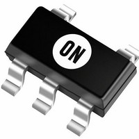
NCP4620DSN15T1G ON Semiconductor, NCP4620DSN15T1G Datasheet - Page 2

NCP4620DSN15T1G
Manufacturer Part Number
NCP4620DSN15T1G
Description
IC REG LDO CMOS 1.5V SOT-23-6
Manufacturer
ON Semiconductor
Datasheet
1.NCP4620DSN15T1G.pdf
(16 pages)
Specifications of NCP4620DSN15T1G
Number Of Outputs
1
Input Voltage Max
12 V
Output Voltage
1.5 V
Output Type
Adjustable
Dropout Voltage (max)
1.1 V
Output Current
165 mA
Load Regulation
5 mV
Voltage Regulation Accuracy
1 %
Maximum Power Dissipation
420 mW
Maximum Operating Temperature
+ 85 C
Mounting Style
SMD/SMT
Package / Case
SOT-23
Minimum Operating Temperature
- 40 C
Regulator Topology
Positive Fixed
Voltage - Output
1.5V
Voltage - Input
2.6 V ~ 10 V
Voltage - Dropout (typical)
-
Number Of Regulators
1
Current - Output
150mA (Min)
Current - Limit (min)
-
Operating Temperature
-40°C ~ 85°C
Mounting Type
Surface Mount
Lead Free Status / RoHS Status
Lead free / RoHS Compliant
Available stocks
Company
Part Number
Manufacturer
Quantity
Price
Company:
Part Number:
NCP4620DSN15T1G
Manufacturer:
ON Semiconductor
Quantity:
2 350
Part Number:
NCP4620DSN15T1G
Manufacturer:
ON/安森美
Quantity:
20 000
Stresses exceeding Maximum Ratings may damage the device. Maximum Ratings are stress ratings only. Functional operation above the
Recommended Operating Conditions is not implied. Extended exposure to stresses above the Recommended Operating Conditions may affect
device reliability.
1. Refer to ELECTRICAL CHARACTERISTIS and APPLICATION INFORMATION for Safe Operating Area.
2. This device series incorporates ESD protection and is tested by the following methods:
VIN
CE
PIN FUNCTION DESCRIPTION
ABSOLUTE MAXIMUM RATINGS
Input Voltage (Note 1)
Output Voltage
Chip Enable Input
Output Current
Power Dissipation − SC−70
Power Dissipation − SOT23
Operating Temperature
Maximum Junction Temperature
Storage Temperature
ESD Capability, Human Body Model (Note 2)
ESD Capability, Machine Model (Note 2)
ESD Human Body Model tested per AEC−Q100−002 (EIA/JESD22−A114)
ESD Machine Model tested per AEC−Q100−003 (EIA/JESD22−A115)
Latchup Current Maximum Rating tested per JEDEC standard: JESD78.
Pin No.
SC−70
5
3
1
4
2
Vref
Thermal Shutdown
NCP4620Hxxxx
Current Limit
Pin No.
SOT23
1
2
3
5
4
Rating
Figure 2. Simplified Schematic Block Diagram
Pin Name
VOUT
GND
VIN
NC
CE
VOUT
http://onsemi.com
GND
Input pin
Ground
Chip enable pin (Active “H”)
Output pin
No connection
VIN
CE
2
Vref
Symbol
ESD
ESD
V
T
I
V
V
OUT
P
Thermal Shutdown
OUT
T
T
STG
CE
IN
A
D
J
HBM
Current Limit
MM
Description
NCP4620Dxxxx
−0.3 to V
−55 to +125
−40 to +85
Value
+150
2000
12.0
12.0
165
380
420
200
IN
+ 0.3
Unit
mW
mA
°C
°C
°C
V
V
V
V
V
VOUT
GND


