BAV74LT3 ON Semiconductor, BAV74LT3 Datasheet

Diodes (General Purpose, Power, Switching) 50V 200mA Dual

BAV74LT3

Manufacturer Part Number
BAV74LT3
Description
Diodes (General Purpose, Power, Switching) 50V 200mA Dual
Manufacturer
ON Semiconductor
Datasheet

Specifications of BAV74LT3

Product
Switching Diodes
Peak Reverse Voltage
50 V
Forward Continuous Current
0.5 A
Max Surge Current
0.5 A
Configuration
Dual Common Cathode
Recovery Time
4 ns
Forward Voltage Drop
1 V
Maximum Reverse Leakage Current
0.1 uA
Maximum Power Dissipation
225 mW
Operating Temperature Range
- 55 C to + 150 C
Maximum Operating Temperature
+ 150 C
Minimum Operating Temperature
- 55 C
Mounting Style
SMD/SMT
Package / Case
SOT-23-3
Lead Free Status / RoHS Status
Lead free / RoHS Compliant

Available stocks

Company
Part Number
Manufacturer
Quantity
Price
Part Number:
BAV74LT3G
Manufacturer:
ON Semiconductor
Quantity:
480
BAV74LT1
Monolithic Dual
Switching Diode
Features
Stresses exceeding Maximum Ratings may damage the device. Maximum
Ratings are stress ratings only. Functional operation above the Recommended
Operating Conditions is not implied. Extended exposure to stresses above the
Recommended Operating Conditions may affect device reliability.
1. FR−5 = 1.0  0.75  0.062 in.
2. Alumina = 0.4  0.3  0.024 in 99.5% alumina.
© Semiconductor Components Industries, LLC, 2006
March, 2006 − Rev. 4
MAXIMUM RATINGS
THERMAL CHARACTERISTICS
Reverse Voltage
Forward Current
Peak Forward Surge Current
Total Device Dissipation FR− 5 Board
(Note 1), T
Derate above 25°C
Thermal Resistance, Junction−to−Ambient
Total Device Dissipation Alumina
Substrate, (Note 2) T
Derate above 25°C
Thermal Resistance, Junction−to−Ambient
Junction and Storage Temperature
Pb−Free Packages are Available
A
= 25°C
Characteristic
Rating
A
= 25°C
(EACH DIODE)
I
Symbol
Symbol
FM(surge)
T
R
R
J
V
P
P
, T
I
qJA
qJA
F
R
D
D
stg
−55 to +150
Value
Max
200
500
225
556
300
417
1.8
2.4
50
1
mW/°C
mW/°C
mAdc
mAdc
°C/W
°C/W
Unit
Unit
mW
mW
Vdc
°C
†For information on tape and reel specifications,
BAV74LT1
BAV74LT1G
BAV74LT3
BAV74LT3G
*Date Code orientation and/or overbar may vary
including part orientation and tape sizes, please
refer to our Tape and Reel Packaging Specifications
Brochure, BRD8011/D.
depending upon manufacturing location.
Device
(Note: Microdot may be in either location)
ORDERING INFORMATION
CATHODE
MARKING DIAGRAM
JA = Device Code
M = Date Code*
G = Pb−Free Package
3
http://onsemi.com
1
SOT−23
(Pb−Free)
(Pb−Free)
Package
SOT−23
SOT−23
SOT−23
1
CASE 318
STYLE 9
SOT−23
JA M G
2
G
Publication Order Number:
3
10,000/Tape & Reel
10,000/Tape & Reel
3000/Tape & Reel
3000/Tape & Reel
ANODE
ANODE
Shipping
1
2
BAV74LT1/D

Related parts for BAV74LT3

BAV74LT3 Summary of contents

Page 1

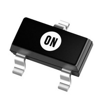
... R 556 qJA P D 300 mW 2.4 mW/°C °C/W R 417 qJA ° −55 to +150 J stg BAV74LT1 BAV74LT1G BAV74LT3 BAV74LT3G †For information on tape and reel specifications, 1 http://onsemi.com ANODE CATHODE ANODE SOT−23 CASE 318 STYLE 9 MARKING DIAGRAM Device Code M = Date Code Pb−Free Package ...

Page 2

ELECTRICAL CHARACTERISTICS Characteristic OFF CHARACTERISTICS Reverse Breakdown Voltage = 5.0 mAdc) (I (BR) Reverse Voltage Leakage Current, (Note Vdc 125° Vdc) R Diode Capacitance ( ...

Page 3

... A A1 *For additional information on our Pb−Free strategy and soldering details, please download the ON Semiconductor Soldering and Mounting Techniques Reference Manual, SOLDERRM/D. ON Semiconductor and are registered trademarks of Semiconductor Components Industries, LLC (SCILLC). SCILLC reserves the right to make changes without further notice to any products herein. SCILLC makes no warranty, representation or guarantee regarding the suitability of its products for any particular purpose, nor does SCILLC assume any liability arising out of the application or use of any product or circuit, and specifically disclaims any and all liability, including without limitation special, consequential or incidental damages. “ ...

Related keywords