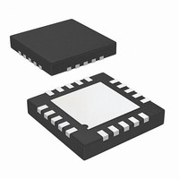
AD7298-1BCPZ Analog Devices Inc, AD7298-1BCPZ Datasheet - Page 14

AD7298-1BCPZ
Manufacturer Part Number
AD7298-1BCPZ
Description
8Channel 10Bit SAR
Manufacturer
Analog Devices Inc
Datasheet
1.AD7298-1BCPZ.pdf
(24 pages)
Specifications of AD7298-1BCPZ
Number Of Bits
10
Sampling Rate (per Second)
1M
Data Interface
Serial, SPI™
Number Of Converters
1
Power Dissipation (max)
23mW
Voltage Supply Source
Single Supply
Operating Temperature
-40°C ~ 125°C
Mounting Type
Surface Mount
Package / Case
20-WFQFN, CSP Exposed Pad
Resolution (bits)
10bit
Sampling Rate
1MSPS
Input Channel Type
Single Ended
Supply Voltage Range - Analog
1.65V To 3.6V
Digital Ic Case Style
LFCSP
Rohs Compliant
Yes
Lead Free Status / RoHS Status
Lead free / RoHS Compliant
Available stocks
Company
Part Number
Manufacturer
Quantity
Price
Company:
Part Number:
AD7298-1BCPZ
Manufacturer:
ADI
Quantity:
200
AD7298-1
ADC Transfer Function
The output coding of the AD7298-1 is straight binary for the
analog input channel conversion results. The designed code
transitions occur at successive LSB values (that is, 1 LSB, 2 LSBs,
and so forth). The LSB size is V
ideal transfer characteristic for the AD7298-1 for straight binary
coding is shown in Figure 22.
V
The AD7298-1 also provides the V
the voltage at which the serial interface operates. V
the ADC to easily interface to both 1.8 V and 3 V processors.
For example, if the AD7298-1 were operated with a V
3.3 V, the V
DRIVE
NOTES
1. V
111...111
111...110
111...000
011...111
REF
000...010
000...001
000...000
IS 2.5V.
DRIVE
Figure 22. Straight Binary Transfer Characteristic
0V
1LSB
pin could be powered from a 1.8 V supply.
ANALOG INPUT
REF
1LSB = V
/1024 for the AD7298-1. The
DRIVE
+V
REF
feature. V
REF
/1024
– 1LSB
DRIVE
DRIVE
DD
controls
allows
of
Rev. A | Page 14 of 24
This enables the AD7298-1 to operate with a larger dynamic
range with a V
1.8 V processors. Take care to ensure V
V
section).
THE INTERNAL OR EXTERNAL REFERENCE
The AD7298-1 can operate with either the internal 2.5 V on-chip
reference or an externally applied reference. The EXT_REF bit
in the control register is used to determine whether the internal
reference is used. If the EXT_REF bit is selected in the control
register, an external reference can be supplied through the V
pin. At power-up, the internal reference is enabled. Suitable
external reference sources for the AD7298-1 include AD780,
AD1582, ADR431, REF193, and ADR391.
The internal reference circuitry consists of a 2.5 V band gap
reference and a reference buffer. When the AD7298-1 is operated
in internal reference mode, the 2.5 V internal reference is
available at the V
using a 10 µF capacitor. It is recommended that the internal
reference be buffered before applying it elsewhere in the system.
The internal reference is capable of sourcing up to 2 mA of current
when the converter is static. The reference buffer requires 5.5 ms to
power up and charge the 10 µF decoupling capacitor during the
power-up time.
DD
by more than 0.3 V (see the Absolute Maximum Ratings
DD
REF
of 3.3 V while still being able to interface to
pin, which should be decoupled to GND1
DRIVE
does not exceed
REF


