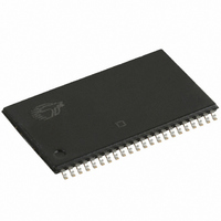
CY7C1049DV33-10ZSXIT Cypress Semiconductor Corp, CY7C1049DV33-10ZSXIT Datasheet - Page 4

CY7C1049DV33-10ZSXIT
Manufacturer Part Number
CY7C1049DV33-10ZSXIT
Description
CY7C1049DV33-10ZSXIT
Manufacturer
Cypress Semiconductor Corp
Specifications of CY7C1049DV33-10ZSXIT
Format - Memory
RAM
Memory Type
SRAM - Asynchronous
Memory Size
4M (512K x 8)
Speed
10ns
Interface
Parallel
Voltage - Supply
3 V ~ 3.6 V
Operating Temperature
-40°C ~ 85°C
Package / Case
44-TSOP II
Memory Configuration
512K X 8
Access Time
10ns
Supply Voltage Range
3V To 3.6V
Memory Case Style
TSOP
No. Of Pins
44
Operating Temperature Range
-40°C To +85°C
Lead Free Status / RoHS Status
Lead free / RoHS Compliant
Available stocks
Company
Part Number
Manufacturer
Quantity
Price
Part Number:
CY7C1049DV33-10ZSXIT
Manufacturer:
CYPRESS/赛普拉斯
Quantity:
20 000
Thermal Resistance
Tested initially and after any design or process changes that may affect these parameters.
AC Test Loads and Waveforms
Data Retention Characteristics
Over the Operating Range
Note
Document Number: 38-05475 Rev. *F
V
I
t
t
3. Tested initially and after any design or process changes that may affect these parameters.
4. AC characteristics (except High Z) are tested using the load conditions shown in
5. No input may exceed V
6. Full device operation requires linear V
CCDR
CDR
R
Parameter
Parameter
DR
[6]
Figure (c).
[3]
JA
JC
V
10 ns device
* CAPACITIVE LOAD CONSISTS
OF ALL COMPONENTS OF THE
TEST ENVIRONMENT
CE
CC
Thermal Resistance
(Junction to Ambient)
Thermal Resistance
(Junction to Case)
V
Data Retention Current
Chip Deselect to Data Retention Time
Operation Recovery Time
CC
OUTPUT
High Z characteristics:
for Data Retention
CC
+ 0.3V.
Description
Description
Z = 50
CC
ramp from V
OUTPUT
3.3V
t
(a)
CDR
Figure 1. AC Test Loads and Waveforms
1.5V
50
3.0V
DR
Figure 2. Data Retention Waveform
to V
Still Air, soldered on a 3 × 4.5 inch,
5 pF
CC(min.)
two layer printed circuit board
(c)
30 pF*
> 50 s or stable at V
V
V
Test Conditions
R 317
CC
IN
DATA RETENTION MODE
> V
= V
CC
351
DR
Figure
V
R2
GND
3.0V
DR
Rise Time: 1 V/ns
– 0.3V or V
= 2.0V, CE > V
> 2V
1. High Z characteristics are tested for all speeds using the test load shown in
CC(min.)
Conditions
IN
> 50 s.
< 0.3V
10%
CC
90%
– 0.3V
[4]
Package
57.91
36.73
[5]
SOJ
ALL INPUT PULSES
3.0V
(b)
t
R
Package
CY7C1049DV33
TSOP II
Auto
Ind’l
50.66
17.17
Fall Time: 1 V/ns
90%
10%
Min
t
2.0
RC
0
Page 4 of 11
Max
10
15
C/W
C/W
Unit
Unit
mA
mA
ns
ns
V
[+] Feedback


