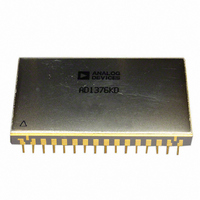
AD1380KD Analog Devices Inc, AD1380KD Datasheet - Page 7

AD1380KD
Manufacturer Part Number
AD1380KD
Description
A/D Converter (A-D) IC
Manufacturer
Analog Devices Inc
Datasheet
1.AD1380JD.pdf
(12 pages)
Specifications of AD1380KD
No. Of Bits
16 Bit
Mounting Type
Through Hole
Features
Low Cost, 16?Bit Sampling ADC
No. Of Channels
1
Interface Type
Serial, Parallel
Package / Case
32-CDIP
Rohs Status
RoHS non-compliant
Number Of Bits
16
Sampling Rate (per Second)
50k
Data Interface
Parallel
Number Of Converters
1
Power Dissipation (max)
900mW
Voltage Supply Source
Dual ±
Operating Temperature
0°C ~ 70°C
Lead Free Status / RoHS Status
DESCRIPTION OF OPERATION
On receipt of a CONVERT START command, the AD1380
converts the voltage at its analog input into an equivalent 16-bit
binary number. This conversion is accomplished as follows: the
16-bit successive-approximation register (SAR) has its 16-bit
outputs connected to both the device bit output pins and the
corresponding bit inputs of the feedback DAC. The analog
input is successively compared to the feedback DAC output, one
bit at a time (MSB first, LSB last). The decision to keep or reject
each bit is then made at the completion of each bit comparison
period, depending on the state of the comparator at that time.
GAIN ADJUSTMENT
The gain adjustment circuit consists of a 100 ppm/°C poten-
tiometer connected across ±V
through a 300 kΩ resistor to Pin 3 (GAIN ADJ) as shown in
Figure 3.
If no external trim adjustment is desired, Pin 5
(COMPARATOR IN) and Pin 3 may be left open.
ZERO OFFSET ADJUSTMENT
The zero offset adjustment circuit consists of a 100 ppm/°C
potentiometer connected across ±V
through a 1.8 MΩ resistor to Pin 5 for all ranges. As shown in
Figure 4, the tolerance of this fixed resistor is not critical; a
carbon composition type is generally adequate. Using a carbon
composition resistor having a −1200 ppm/°C temperature
coefficient contributes a worst-case offset temperature
coefficient of 32 LSB
2.3 ppm/°C of FSR, if the offset adjustment potentiometer is set
at either end of its adjustment range. Since the maximum offset
adjustment required is typically no more than ±16 LSB
a carbon composition offset summing resistor typically
contributes no more than 1 ppm/°C of FSR offset temperature
coefficient.
An alternate offset adjustment circuit, which contributes a
negligible offset temperature coefficient if metal film resistors
(temperature coefficient <100 ppm/°C) are used, is shown in
Figure 5.
Figure 4. Zero Offset Adjustment Circuit (±0.3% FSR)
100ppm/°C
Figure 3. Gain Adjustment Circuit (±0.2% FSR)
100kΩ
10kΩ
TO
+15V
–15V
100kΩ
10kΩ
14
B
TO
× 61 ppm/LSB
+15V
–15V
1.8MΩ
300kΩ
0.01μF
S
with its slider connected
5
AD1380
S
14
B
3
with its slider connected
× 1200 ppm/°C =
AD1380
14
B
, use of
Rev. D | Page 7 of 12
In either adjustment circuit, the fixed resistor connected to
Pin 5 should be located close to this pin to keep the pin
connection runs short. Pin 5 is quite sensitive to external noise
pickup and should be guarded by ANALOG COMMON.
TIMING
The timing diagram is shown in Figure 6. Receipt of a
CONVERT START signal sets the STATUS flag, indicating
conversion in progress. This, in turn, removes the inhibit
applied to the gated clock, permitting it to run through
17 cycles. All the SAR parallel bits, STATUS flip-flops and the
gated clock inhibit signal are initialized on the trailing edge of
the CONVERT START signal. At time t
B
(keep) and Bit 2 is reset unconditionally. This sequence
continues until the Bit 16 (LSB) decision (keep) is made at t
The STATUS flag is reset, indicating that the conversion is
complete and the parallel output data is valid. Resetting the
STATUS flag restores the gated clock inhibit signal, forcing the
clock output to the low Logic 0 state. Note that the clock
remains low until the next conversion.
Corresponding parallel data bits become valid on the same
positive-going clock edge.
INTERNAL
CONVERT
STATUS
16
CLOCK
START
BIT 10
BIT 11
BIT 12
BIT 13
BIT 14
BIT 15
BIT 2
BIT 3
BIT 4
BIT 5
BIT 6
BIT 7
BIT 8
BIT 9
are set unconditionally. At t
MSB
LSB
Figure 5. Low Temperature Coefficient Zero Adjustment Circuit
(1)
OFFSET
NOTES:
Figure 6. Timing Diagram (Binary Code 0110011101 111010)
1. THE CONVERT START PULSEWIDTH IS 50ns MIN AND MUST REMAIN LOW DURING A
2.
3. MSB DECISION.
4. CLOCK REMAINS LOW AFTER LAST BIT DECISION.
CONVERSION. THE CONVERSION IS INITIATED BY THE TRAILING EDGE OF THE
CONVERT COMMAND.
t
CONV
t
ADJ
0
0
MSB
(3)
= 14μs (MAX),
t
0
1
100kΩ
10kΩ
t
1
1
2
TO
+15V
–15V
t
1
1
3
t
t
0
0
180kΩ M.F. 180kΩ M.F.
ACQ
4
t
MAXIMUM THROUGHPUT TIME
5
0
0
= 6μs (MAX).
CONVERSION TIME (2)
t
1
1
6
t
1
1
7
1
22kΩ M.F.
, the Bit 1 decision is made
t
1
1
8
t
9
0
0
t
10
1
1
0
, B
t
11
1
1
5
1
t
12
1
1
is reset and B
AD1380
t
13
1
1
t
14
0
0
t
15
1
1
AD1380
t
t
(4)
0
0
ACQUISITION
16
t
2
17
to
16
LSB
.


