AD1865N-K Analog Devices Inc, AD1865N-K Datasheet - Page 4
AD1865N-K
Manufacturer Part Number
AD1865N-K
Description
IC, DUAL 18-BIT AUDIO DAC
Manufacturer
Analog Devices Inc
Datasheet
1.AD1865N-J.pdf
(12 pages)
Specifications of AD1865N-K
Rohs Status
RoHS non-compliant
Number Of Bits
18
Data Interface
Serial
Number Of Converters
2
Voltage Supply Source
Analog and Digital, Dual ±
Power Dissipation (max)
260mW
Operating Temperature
-25°C ~ 70°C
Mounting Type
Through Hole
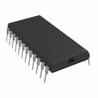
Package / Case
24-DIP (0.600", 15.24mm)
Settling Time
-
Lead Free Status / RoHS Status
Available stocks
Company
Part Number
Manufacturer
Quantity
Price


AD1865
TOTAL HARMONIC DISTORTION + NOISE
Total harmonic distortion plus noise (THD+N) is defined as
the ratio of the square root of the sum of the squares of the am-
plitudes of the harmonics and noise to the value of the funda-
mental input frequency. It is usually expressed in percent.
THD+N is a measure of the magnitude and distribution of lin-
earity error, differential linearity error, quantization error and
noise. The distribution of these errors may be different, depend-
ing on the amplitude of the output signal. Therefore, to be most
useful, THD+N should be specified for both large (0 dB) and
small (–20 dB, –60 dB) signal amplitudes. THD+N measure-
ments for the AD1865 are made using the first 19 harmonics
and noise out to 30 kHz.
SIGNAL-TO-NOISE RATIO
The signal-to-noise ratio is defined as the ratio of the amplitude
of the output when a full-scale code is entered to the amplitude
of the output when a midscale code is entered. It is measured
using a standard A-Weight filter. SNR for the AD1865 is mea-
sured for noise components out to 30 kHz.
CHANNEL SEPARATION
Channel separation is defined as the ratio of the amplitude of a
full-scale signal appearing on one channel to the amplitude of
that same signal which couples onto the adjacent channel. It is
usually expressed in dB. For the AD1865 channel separation is
measured in accordance with EIAJ Standard CP-307, Section
5.5.
D-RANGE DISTORTION
D-Range distortion is equal to the value of the total harmonic
distortion + noise (THD+N) plus 60 dB when a signal level of
–60 dB below full scale is reproduced. D-Range is tested with a
1 kHz input sine wave. This is measured with a standard A-Weight
filter as specified by EIAJ Standard CP-307.
GAIN ERROR
The gain error specification indicates how closely the output of
a given channel matches the ideal output for given input data. It
is expressed in % of FSR and is measured with a full-scale out-
put signal.
INTERCHANNEL GAIN MATCHING
The gain matching specification indicates how closely the ampli-
tudes of the output signals match when producing identical in-
put data. It is expressed in % of FSR (Full-Scale Range = 6 V
for the AD1865) and is measured with full-scale output signals.
MIDSCALE ERROR
Midscale error is the deviation of the actual analog output of a
given channel from the ideal output (0 V) when the twos
complement input code representing half scale is loaded into the
input register of the DAC. It is expressed in mV and is mea-
sured with half-scale output signals.
–4–
INTERCHANNEL MIDSCALE MATCHING
The midscale matching specification indicates how closely the
amplitudes of the output signals of the two channels match
when the twos complement input code representing half scale is
loaded into the input register of both channels. It is expressed in
mV and is measured with half-scale output signals.
FUNCTIONAL DESCRIPTION
The AD1865 is a complete, monolithic, dual 18-bit audio DAC.
No external components are required for operation. As shown in
the block diagram, each chip contains two voltage references,
two output amplifiers, two 18-bit serial input registers and two
18-bit DACs.
The voltage reference section provides a reference voltage for
each DAC circuit. These voltages are produced by low-noise
bandgap circuits. Buffer amplifiers are also included. This com-
bination of elements produces reference voltages that are unaf-
fected by changes in temperature and age.
The output amplifiers use both MOS and bipolar devices and
incorporate an all NPN output stage. This design technique
produces higher slew rate and lower distortion than previous
techniques. Frequency response is also improved. When com-
bined with the appropriate on-chip feedback resistor, the output
op amps convert the output current to output voltages.
The 18-bit D/A converters use a combination of segmented de-
coder and R-2R architecture to achieve consistent linearity and
differential linearity. The resistors which form the ladder struc-
ture are fabricated with silicon chromium thin film. Laser trim-
ming of these resistors further reduces linearity errors resulting
in low output distortion.
The input registers are fabricated with CMOS logic gates.
These gates allow the achievement of fast switching speeds and
low power consumption, contributing to the low glitch and low
power dissipation of the AD1865.
TRIM
AGND
MSB
V
–V
I
CLK
OUT
+V
OUT
DR
R
LR
SJ
S
F
L
AD1865 Block Diagram (DIP Package)
10
11
12
4
1
2
3
5
6
7
8
9
LATCH
18-BIT
REFERENCE
NC = NO CONNECT
18-BIT
D/A
AD1865
18-BIT
D/A
REFERENCE
LATCH
18-BIT
22
20
19
18
17
16
15
14
13
24
23
21
+V
TRIM
I
SJ
R
DL
MSB
V
NC
AGND
LL
DGND
OUT
F
OUT
S
REV. 0
Related parts for AD1865N-K
Image
Part Number
Description
Manufacturer
Datasheet
Request
R

Part Number:
Description:
±1.7g Dual-Axis IMEMS Accelerometer Evaluation Board
Manufacturer:
Analog Devices Inc
Datasheet:

Part Number:
Description:
Inertial Sensor Evaluation System
Manufacturer:
Analog Devices Inc
Datasheet:
Part Number:
Description:
Manufacturer:
Analog Devices Inc
Datasheet:
Part Number:
Description:
Manufacturer:
Analog Devices Inc
Datasheet:
Part Number:
Description:
Manufacturer:
Analog Devices Inc
Datasheet:
Part Number:
Description:
Manufacturer:
Analog Devices Inc
Datasheet:
Part Number:
Description:
Manufacturer:
Analog Devices Inc
Datasheet:
Part Number:
Description:
Manufacturer:
Analog Devices Inc
Datasheet:
Part Number:
Description:
Manufacturer:
Analog Devices Inc
Datasheet:
Part Number:
Description:
Manufacturer:
Analog Devices Inc
Datasheet:
Part Number:
Description:
Manufacturer:
Analog Devices Inc
Datasheet:
Part Number:
Description:
Manufacturer:
Analog Devices Inc
Datasheet:
Part Number:
Description:
Manufacturer:
Analog Devices Inc
Datasheet: