AD2S80ATD Analog Devices Inc, AD2S80ATD Datasheet - Page 5
AD2S80ATD
Manufacturer Part Number
AD2S80ATD
Description
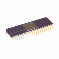
Motion And Motor Control, Resolver To Digital Converter, 16 Bit Interface, AD2S80, 40 Lead, Ceramic DIP
Manufacturer
Analog Devices Inc
Type
R/D Converterr
Specifications of AD2S80ATD
Rohs Status
RoHS non-compliant
Input Type
Parallel
Output Type
Digital
Interface
Parallel
Current - Supply
30mA
Mounting Type
Through Hole
Package / Case
40-CDIP (0.600", 15.24mm)
Lead Free Status / RoHS Status
Available stocks
Company
Part Number
Manufacturer
Quantity
Price

Company:
Part Number:
AD2S80ATD
Manufacturer:
ADI
Quantity:
835
Company:
Part Number:
AD2S80ATD-883B
Manufacturer:
AD
Quantity:
2
Company:
Part Number:
AD2S80ATD/883B
Manufacturer:
EPCOS
Quantity:
1 001
Company:
Part Number:
AD2S80ATD/883B
Manufacturer:
ADI
Quantity:
685


RECOMMENDED OPERATING CONDITIONS
Power Supply Voltage (+V
Power Supply Voltage V
Analog Input Voltage (SIN and COS) . . . . . . . . 2 V rms ± 10%
Analog Input Voltage (REF) . . . . . . . . . . . . . . 1 V to 8 V peak
Signal and Reference Harmonic Distortion . . . . . . . 10% (max)
Phase Shift Between Signal and Reference . . . ± 10 Degrees (max)
Ambient Operating Temperature Range
ABSOLUTE MAXIMUM RATINGS
+V
–V
+V
Reference . . . . . . . . . . . . . . . . . . . . . . . . . . . . . . . . 14 V to –V
SIN . . . . . . . . . . . . . . . . . . . . . . . . . . . . . . . . . . . . 14 V to –V
COS . . . . . . . . . . . . . . . . . . . . . . . . . . . . . . . . . . . 14 V to –V
Any Logical Input . . . . . . . . . . . . . . . . . . . –0.4 V dc to +V
Demodulator Input . . . . . . . . . . . . . . . . . . . . . . . . 14 V to –V
Integrator Input . . . . . . . . . . . . . . . . . . . . . . . . . . . 14 V to –V
VCO Input . . . . . . . . . . . . . . . . . . . . . . . . . . . . . . 14 V to –V
Power Dissipation . . . . . . . . . . . . . . . . . . . . . . . . . . . . 860 mW
Operating Temperature
θ
θ
Storage Temperature (All Grades) . . . . . . . . –65°C to +150°C
Lead Temperature (Soldering, 10 sec) . . . . . . . . . . . . . 300°C
CAUTION NOTES:
1
2
3
Absolute Maximum Ratings are those values beyond which damage to the device
Correct polarity voltages must be maintained on the +V
With reference to Appendix C of MIL-M-38510.
may occur.
Binary
Bits (N)
JC
JC
10
11
12
13
14
15
16
17
18
Commercial (JD, KD, LD) . . . . . . . . . . . . . . . . 0°C to 70°C
Industrial (AD, BD) . . . . . . . . . . . . . . . . . . . –40°C to +85°C
Extended (SD, SE, TD, TE, UD, UE) . . . –55°C to +125°C
Commercial (JD, KD, LD) . . . . . . . . . . . . . . . . 0°C to 70°C
Industrial (AD, BD) . . . . . . . . . . . . . . . . . . . –40°C to +85°C
Extended (SD, SE, TD, TE, UD, UE) . . . –55°C to +125°C
5
6
7
8
9
0
1
2
3
4
S
3
3
S
L
2
(40-Lead DIP 883 Parts Only) . . . . . . . . . . . . . . . 11°C/W
(44-Terminal LCC 883 Parts Only) . . . . . . . . . . . 10°C/W
. . . . . . . . . . . . . . . . . . . . . . . . . . . . . . . . . . . . . . –14 V dc
. . . . . . . . . . . . . . . . . . . . . . . . . . . . . . . . . . . . . . . . . . . V
. . . . . . . . . . . . . . . . . . . . . . . . . . . . . . . . . . . . . +14 V dc
Resolution
(2
116384
131072
262144
32768
65536
N
1024
2048
4096
8192
)
128
256
512
16
32
64
1
2
4
8
Bit Weight Table
Degrees
/Bit
360.0
180.0
L
90.0
45.0
22.5
11.25
5.625
2.8125
1.40625
0.703125
0.3515625
0.1757813
0.0878906
0.0439453
0.0219727
0.0109836
0.0054932
0.0027466
0.0013733
. . . . . . . . . . . . . . . . . . . 5 V dc ± 10%
S
, –V
S
) . . . . . . . . . ± 12 V dc ± 10%
Minutes
/Bit
21600.0
10800.0
l
5400.0
2700.0
1350.0
675.0
337.5
168.75
(
with respect to GND
84.375
42.1875
21.09375
10.546875
5.273438
2.636719
1.318359
0.659180
0.329590
0.164795
0.082397
S
and –V
Seconds
/Bit
1296000.0
324000.0
162000.0
648000.0
S
81000.0
40500.0
20250.0
10125.0
pins.
5062.5
2531.25
1265.625
632.8125
316.40625
158.20313
79.10156
39.55078
19.77539
9.88770
4.94385
)
L
dc
S
S
S
S
S
S
S
MSB DB1
DIP (D) Package
DB5
DB2
DB3
DB4
DB6
DB7
DB8
+V
SIN
NC
S
NC = NO CONNECT
10
11
12
13
14
15
16
17
7
8
9
ENABLE
INHIBIT
18 19
6
5
4
20
3
21
(Not to Scale)
AD2S80A
PIN CONFIGURATIONS
TOP VIEW
2
22
PIN DESIGNATIONS
1
23
44 43 42 41 40
24
REFERENCE I/P
AC ERROR O/P
ANALOG GND
SIGNAL GND
25
DEMOD I/P
26
MSB DB1
27
DB10
DB11
DB12
COS
DB2
DB3
DB4
DB5
DB6
DB7
DB8
DB9
+V
SIN
28
S
10
11
12
13
14
15
16
17
18
19
20
4
1
2
3
5
6
7
8
9
39
38
37
36
35
34
33
32
31
30
29
(Not to Scale)
AD2S80A
TOP VIEW
INHIBIT
–V
RIPPLE CLOCK
DIRECTION
BUSY
DATA LOAD
NC
SC2
SC1
DIGITAL GND
NC
LCC (E) Package
S
AD2S80A
40
39
38
37
36
35
34
33
32
31
30
29
28
27
26
25
24
23
22
21
INHIBIT
DEMOD O/P
INTEGRATOR O/P
INTEGRATOR I/P
VCO I/P
–V
RIPPLE CLK
DIRECTION
BUSY
DATA LOAD
SC2
SC1
DIGITAL GND
BYTE SELECT
ENABLE
V
DB16 LSB
DB15
DB14
DB13
L
S
Related parts for AD2S80ATD
Image
Part Number
Description
Manufacturer
Datasheet
Request
R

Part Number:
Description:
±1.7g Dual-Axis IMEMS Accelerometer Evaluation Board
Manufacturer:
Analog Devices Inc
Datasheet:

Part Number:
Description:
Inertial Sensor Evaluation System
Manufacturer:
Analog Devices Inc
Datasheet:
Part Number:
Description:
Manufacturer:
Analog Devices Inc
Datasheet:
Part Number:
Description:
Manufacturer:
Analog Devices Inc
Datasheet:
Part Number:
Description:
Manufacturer:
Analog Devices Inc
Datasheet:
Part Number:
Description:
Manufacturer:
Analog Devices Inc
Datasheet:
Part Number:
Description:
Manufacturer:
Analog Devices Inc
Datasheet:
Part Number:
Description:
Manufacturer:
Analog Devices Inc
Datasheet:
Part Number:
Description:
Manufacturer:
Analog Devices Inc
Datasheet:
Part Number:
Description:
Manufacturer:
Analog Devices Inc
Datasheet:
Part Number:
Description:
Manufacturer:
Analog Devices Inc
Datasheet:
Part Number:
Description:
Manufacturer:
Analog Devices Inc
Datasheet:
Part Number:
Description:
Manufacturer:
Analog Devices Inc
Datasheet: