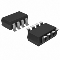
AD5171BRJZ100-R2 Analog Devices Inc, AD5171BRJZ100-R2 Datasheet - Page 19

AD5171BRJZ100-R2
Manufacturer Part Number
AD5171BRJZ100-R2
Description
IC,Digital Potentiometer,CMOS,TSSOP,8PIN,PLASTIC
Manufacturer
Analog Devices Inc
Datasheet
1.AD5171BRJZ10-R7.pdf
(24 pages)
Specifications of AD5171BRJZ100-R2
Taps
64
Resistance (ohms)
100K
Number Of Circuits
1
Temperature Coefficient
35 ppm/°C Typical
Memory Type
Non-Volatile
Interface
I²C, 2-Wire Serial
Voltage - Supply
2.7 V ~ 5.5 V
Operating Temperature
-40°C ~ 125°C
Mounting Type
Surface Mount
Package / Case
SOT-23-8
Resistance In Ohms
100K
Lead Free Status / RoHS Status
Lead free / RoHS Compliant
For Use With
AD5171EVAL - BOARD EVAL FOR AD5171
Lead Free Status / RoHS Status
Lead free / RoHS Compliant
Other names
AD5171BRJZ100R2TR
APPLICATIONS INFORMATION
DAC
It is common to buffer the output of the digital potentiometer as
a DAC unless the load is much larger than R
impede conversion and deliver higher current, if needed.
GAIN CONTROL COMPENSATION
The digital potentiometers are commonly used in gain
controls or sensor transimpedance amplifier signal conditioning
applications (see Figure 40). To avoid gain peaking, or in worst-
case oscillation due to step response, a compensation capacitor
is needed. In general, C2 in the range of a few picofarads to a
few tenths of a picofarad is adequate for the compensation.
PROGRAMMABLE VOLTAGE SOURCE WITH
BOOSTED OUTPUT
For applications that require high current adjustment, such as a
laser diode driver or tunable laser, a boosted voltage source can
be considered (see Figure 41).
AD5171
Figure 39. Programmable Voltage Reference (DAC)
U1
Figure 41. Programmable Booster Voltage Source
Figure 40. Typical Noninverting Gain Amplifier
V
V
GND
IN
1
2
AD1582
5V
OUT
A
B
U1
W
47kΩ
V
R1
IN
AD8601
3
V
+V
AD5171
I
–V
U2
A
B
B
U3 2N7002
R2 100kΩ
W
4.7pF
A1
C2
U1
W
AD8601
5V
A
SIGNAL
U2
V
WB
O
LD
C
C
. The buffer can
V
O
R
BIAS
V
OUT
I
L
Rev. D | Page 19 of 24
In this circuit, the inverting input of the op amp forces the V
to be equal to the wiper voltage set by the digital potentiometer.
The load current is then delivered by the supply via the N‒Ch
FET N
(V
100 mA with a 5 V supply. For precision applications, a voltage
reference, such as the ADR421, ADR03, or ADR370, can be
applied at Terminal A of the digital potentiometer.
LEVEL SHIFTING FOR DIFFERENT VOLTAGE
OPERATION
If the SCL and SDA signals come from a low voltage logic
controller and are below the minimum V
level shift the signals for read/write communications between
the AD5171 and the controller. Figure 42 shows one of the
implementations. For example, when SDA1 is at 2.5 V, M1 turns
off, and SDA2 becomes 5 V. When SDA1 is at 0 V, M1 turns on,
and SDA2 approaches 0 V. As a result, proper level shifting is
established. M1 and M2 should be low threshold N-Ch power
MOSFETs, such as FDV301N.
SDA1
SCL1
RESISTANCE SCALING
The AD5171 offers 5 kΩ, 10 kΩ, 50 kΩ, and 100 kΩ nominal
resistances. For users who need to optimize the resolution with
an arbitrary full range resistance, the following techniques can
be used. By paralleling a discrete resistor, a proportionately lower
voltage appears at Terminal A to Terminal B, which is applicable
only to the voltage divider mode (see Figure 43).
This translates into a finer degree of precision because the step
size at Terminal W is smaller. The voltage can be found as
V
I
DD1
− V
V
CONTROLLER
= 2.5V
W
1
. N
O
(
) × I
Figure 42. Level Shifting for Different Voltage Operation
D
2.5V
1
)
power handling must be adequate to dissipate
=
L
Figure 43. Lowering the Nominal Resistance
power. This circuit can source a maximum of
Rp
R3
(
R
+
AB
R
AB
||
Rp
R2
S
||
R2
M1
R2
)
G
×
V
R1
DD
64
R3
D
D
A
B
S
M2
×
G
V
W
DD
D
Rp
IH
level (0.7 V × V
Rp
2.7V–5.5V
AD5171
V
AD5171
DD2
= 5V
SDA2
SCL2
DD
OUT
),
(5)


