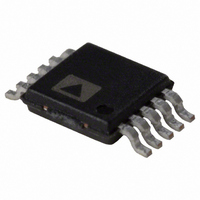
AD5258BRMZ10-R7 Analog Devices Inc, AD5258BRMZ10-R7 Datasheet - Page 5

AD5258BRMZ10-R7
Manufacturer Part Number
AD5258BRMZ10-R7
Description
IC,Digital Potentiometer,TSSOP,10PIN,PLASTIC
Manufacturer
Analog Devices Inc
Datasheet
1.AD5258BRMZ100.pdf
(24 pages)
Specifications of AD5258BRMZ10-R7
Taps
64
Resistance (ohms)
10K
Number Of Circuits
1
Temperature Coefficient
200 ppm/°C Typical
Memory Type
Non-Volatile
Interface
I²C, 2-Wire Serial
Voltage - Supply
2.7 V ~ 5.5 V
Operating Temperature
-40°C ~ 85°C
Mounting Type
Surface Mount
Package / Case
10-MSOP, Micro10™, 10-uMAX, 10-uSOP
Resistance In Ohms
10K
Lead Free Status / RoHS Status
Lead free / RoHS Compliant
For Use With
AD5258EVAL - BOARD EVAL FOR AD5258 DGTL POT
Lead Free Status / RoHS Status
Lead free / RoHS Compliant
Available stocks
Company
Part Number
Manufacturer
Quantity
Price
Part Number:
AD5258BRMZ10-R7
Manufacturer:
ADI/亚德诺
Quantity:
20 000
TIMING CHARACTERISTICS
V
Table 2.
Parameter
I
FLASH/EE MEMORY RELIABILITY
1
2
3
4
2
During power-up, the output is momentarily preset to midscale before restoring EEPROM content.
Delay time after power-on preset prior to writing new EEPROM data.
Endurance is qualified to 100,000 cycles per JEDEC Std. 22 Method A117 and is measured at −40°C, +25°C, and +85°C; typical endurance at +25°C is 700,000 cycles.
Retention lifetime equivalent at junction temperature (T
with junction temperature.
C INTERFACE TIMING CHARACTERISTICS
DD
SCL Clock Frequency
t
t
t
t
t
t
t
t
t
t
EEPROM Data Storing Time
EEPROM Data Restoring Time at Power On
EEPROM Data Restoring Time upon Restore
EEPROM Data Rewritable Time
Endurance
Data Retention
BUF
HD;STA
LOW
HIGH
SU;STA
HD;DAT
SU;DAT
F
R
SU;STO
Command
= V
Fall Time of Both SDA and SCL Signals
Rise Time of Both SDA and SCL Signals
Bus-Free Time Between Stop and Start
Low Period of SCL Clock
High Period of SCL Clock
LOGIC
Setup Time for Repeated Start Condition
Hold Time (Repeated start)
Data Setup Time
Setup Time for Stop Condition
Data Hold Time
= 5 V ± 10%, or 3 V ± 10%; V
3
1
SDA
SCL
4
P
t
1
2
S
t
2
A
t
3
= V
1
J
) = 55°C per JEDEC Std. 22, Method A117. Retention lifetime based on an activation energy of 0.6 eV derates
DD
t
; V
Symbol
f
t
t
t
t
t
t
t
t
t
t
t
t
t
t
8
SCL
1
2
3
4
5
6
7
8
9
10
EEMEM_STORE
EEMEM_RESTORE1
EEMEM_RESTORE2
EEMEM_REWRITE
t
8
Figure 3. I
B
t
9
= 0 V; −40°C < T
Rev. C | Page 5 of 24
2
C Interface Timing Diagram
t
9
Conditions
After this period, the first clock pulse is
generated.
V
out decoupling capacitors at V
V
t
4
DD
DD
rise time dependant. Measure with-
= 5 V.
A
< +85°C, unless otherwise noted.
t
5
t
7
t
DD
6
and GND.
Min
0
1.3
0.6
1.3
0.6
0.6
0
100
0.6
100
P
Typ
26
300
300
540
700
100
t
10
Max
400
0.9
300
300
AD5258
Unit
kHz
μs
μs
μs
μs
μs
μs
ns
ns
ns
μs
ms
μs
μs
μs
kCycles
Years


