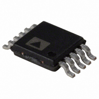
AD5426YRM Analog Devices Inc, AD5426YRM Datasheet - Page 4

AD5426YRM
Manufacturer Part Number
AD5426YRM
Description
8-IOUT DAC WITH SERIAL ITF I.C.
Manufacturer
Analog Devices Inc
Datasheet
1.AD5443YRMZ.pdf
(28 pages)
Specifications of AD5426YRM
Rohs Compliant
NO
Rohs Status
RoHS non-compliant
Design Resources
Unipolar, Precision DC Digital-to-Analog Conversion Using AD5426/32/43 8-Bit to12-Bit DACs (CN0034) Precision, Bipolar Configuration for the AD5426/32/43 8-Bit to12-Bit DACs (CN0036) AC Signal Processing Using AD5426/32/43 Current Output DACs (CN0037) Programmable Gain Element Using AD5426/32/43 Current Output DACs (CN0038)
Number Of Bits
8
Data Interface
Serial
Number Of Converters
1
Voltage Supply Source
Single Supply
Operating Temperature
-40°C ~ 125°C
Mounting Type
Surface Mount
Package / Case
10-MSOP, Micro10™, 10-uMAX, 10-uSOP
Power Dissipation (max)
25µW
Settling Time
50ns
Lead Free Status / RoHS Status
Available stocks
Company
Part Number
Manufacturer
Quantity
Price
Part Number:
AD5426YRM
Manufacturer:
ADI/亚德诺
Quantity:
20 000
Company:
Part Number:
AD5426YRMZ
Manufacturer:
MAX
Quantity:
26
Part Number:
AD5426YRMZ
Manufacturer:
ADI/亚德诺
Quantity:
20 000
AD5426/AD5432/AD5443
Parameter
Output Capacitance
POWER REQUIREMENTS
1
Guaranteed by design and characterization, not subject to production testing.
Digital Feedthrough
Analog THD
Digital THD
Output Noise Spectral Density
SFDR Performance (Wide Band)
SFDR Performance (Narrow Band)
Power Supply Range
I
Power Supply Sensitivity
I
I
Intermodulation Distortion
DD
OUT
OUT
50 kHz f
20 kHz f
20 kHz f
50 kHz f
50 kHz f
20 kHz f
1
2
OUT
OUT
OUT
OUT
OUT
OUT
1
Min
3.0
0.1
78
Typ
12
10
22
10
81
73
74
25
75
76
87
87
0.4
Max
17
12
25
12
5.5
0.6
5
0.001
Rev. C | Page 4 of 28
Unit
pF
pF
pF
pF
nV-s
dB
dB
dB
nV/√Hz
dB
dB
dB
dB
dB
V
μA
μA
%/%
Clock = 1 MHz, V
Clock = 1 MHz, V
Clock = 1 MHz, V
Clock = 1 MHz, f
T = −40°C to +125°C , logic inputs = 0 V or V
Conditions
All 0s loaded
All 1s loaded
All 0s loaded
All 1s loaded
Feedthrough to DAC output with SYNC high and
alternate loading of all 0s and all 1s
V
@ 1 kHz
T
∆V
A
REF
= 25°C, logic inputs = 0 V or V
DD
= 3.5 V p-p, all 1s loaded, f = 1 kHz
= ±5%
1
REF
REF
REF
= 20 kHz, f
= 3.5 V, C
= 3.5 V
= 3.5 V
2
COMP
= 25 kHz, V
DD
= 1.8 pF
REF
= 3.5 V
DD


