AD5532ABC-2 Analog Devices Inc, AD5532ABC-2 Datasheet - Page 6
AD5532ABC-2
Manufacturer Part Number
AD5532ABC-2
Description
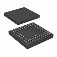
IC,Sample/Track-and-Hold Amplifier,32-CHANNEL,CMOS,BGA,74PIN,PLASTIC
Manufacturer
Analog Devices Inc
Specifications of AD5532ABC-2
Rohs Status
RoHS non-compliant
Settling Time
30µs
Number Of Bits
14
Data Interface
Serial
Number Of Converters
34
Voltage Supply Source
Analog and Digital
Power Dissipation (max)
623mW
Operating Temperature
-40°C ~ 85°C
Mounting Type
Surface Mount
Package / Case
74-CSPBGA
Number Of Channels
32
Resolution
14b
Conversion Rate
45KSPS
Interface Type
PARALLEL/SERIAL 3W
Single Supply Voltage (typ)
Not RequiredV
Dual Supply Voltage (typ)
±9/5/±12/5/±15/5V
Power Supply Requirement
Dual
Output Type
Voltage
Single Supply Voltage (min)
Not RequiredV
Single Supply Voltage (max)
Not RequiredV
Dual Supply Voltage (min)
-4.75/8/4.75V
Dual Supply Voltage (max)
±16.5/5.25V
Operating Temp Range
-40C to 85C
Operating Temperature Classification
Industrial
Mounting
Surface Mount
Pin Count
74
For Use With
EVAL-AD5532HSEBZ - BOARD EVAL FOR AD5532HSEVAL-AD5532EBZ - BOARD EVAL FOR AD5532
Lead Free Status / Rohs Status
Not Compliant
Available stocks
Company
Part Number
Manufacturer
Quantity
Price
Company:

Part Number:
AD5532ABC-2
Manufacturer:
AD
Quantity:
1 831
Company:
Part Number:
AD5532ABC-2
Manufacturer:
ADI
Quantity:
150
Company:
Part Number:
AD5532ABC-2
Manufacturer:
Analog Devices Inc
Quantity:
10 000


AD5532
TIMING CHARACTERISTICS
PARALLEL INTERFACE
Table 3.
Parameter
t
t
t
t
t
t
1
2
PARALLEL INTERFACE TIMING DIAGRAMS
A4–A0, CAL,
1
2
3
4
5
6
See Figure 2 and Figure 3, the parallel interface timing diagrams.
Guaranteed by design and characterization, not production tested.
OFFS_SEL
WR
CS
1, 2
Figure 2. Parallel Write (ISHA Mode Only)
t
1
Limit at T
0
0
50
50
20
7
t
t
3
4
t
5
MIN
, T
MAX
t
2
t
6
(A Version)
Rev. D | Page 6 of 20
Unit
ns min
ns min
ns min
ns min
ns min
ns min
Conditions/Comments
CS to WR setup time
CS to WR hold time
CS pulse width low
WR pulse width low
A4–A0, CAL, OFFS_SEL to WR setup time
A4–A0, CAL, OFFS_SEL to WR hold time
Figure 3. Load Circuit for D
TO OUTPUT
PIN
50pF
C
L
200μA
200μA
OUT
Timing Specifications
I
I
OL
OH
1.6V
Related parts for AD5532ABC-2
Image
Part Number
Description
Manufacturer
Datasheet
Request
R

Part Number:
Description:
Cmos, 330 Mhz Triple 8-bit High Speed Video Dac
Manufacturer:
Analog Devices, Inc.
Datasheet:

Part Number:
Description:
±1.7g Dual-Axis IMEMS Accelerometer Evaluation Board
Manufacturer:
Analog Devices Inc
Datasheet:

Part Number:
Description:
Inertial Sensor Evaluation System
Manufacturer:
Analog Devices Inc
Datasheet:
Part Number:
Description:
Manufacturer:
Analog Devices Inc
Datasheet:
Part Number:
Description:
Manufacturer:
Analog Devices Inc
Datasheet:
Part Number:
Description:
Manufacturer:
Analog Devices Inc
Datasheet:
Part Number:
Description:
Manufacturer:
Analog Devices Inc
Datasheet:
Part Number:
Description:
Manufacturer:
Analog Devices Inc
Datasheet:
Part Number:
Description:
Manufacturer:
Analog Devices Inc
Datasheet:
Part Number:
Description:
Manufacturer:
Analog Devices Inc
Datasheet:
Part Number:
Description:
Manufacturer:
Analog Devices Inc
Datasheet:
Part Number:
Description:
Manufacturer:
Analog Devices Inc
Datasheet:
Part Number:
Description:
Manufacturer:
Analog Devices Inc
Datasheet: