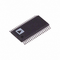
AD5557CRU-REEL7 Analog Devices Inc, AD5557CRU-REEL7 Datasheet - Page 8

AD5557CRU-REEL7
Manufacturer Part Number
AD5557CRU-REEL7
Description
IC,D/A CONVERTER,DUAL,14-BIT,TSSOP,38PIN
Manufacturer
Analog Devices Inc
Datasheet
1.AD5547BRUZ.pdf
(20 pages)
Specifications of AD5557CRU-REEL7
Design Resources
Precision, Unipolar, Inverting Conversion Using AD5547/57 DAC (CN0026) Precision, Unipolar, Noninverting Configuration for the AD5547/57 DAC (CN0027) Precision, Bipolar, Configuration for AD5547/AD5557 DAC (CN0028)
Settling Time
500ns
Number Of Bits
14
Data Interface
Parallel
Number Of Converters
2
Voltage Supply Source
Single Supply
Power Dissipation (max)
55µW
Operating Temperature
-40°C ~ 125°C
Mounting Type
Surface Mount
Package / Case
38-TSSOP
Lead Free Status / RoHS Status
Contains lead / RoHS non-compliant
AD5547/AD5557
Table 4. AD5557 Pin Function Descriptions
Pin No.
1, 2
3
4
5
6
7
8
9
10
11
12
13
14
15
16
17
18
19
20
21
22
Mnemonic
NC
R
R
R
R
V
I
AGNDA
DGND
AGNDB
I
V
R
R
R
R
WR
A0
A1
LDAC
MSB
OUTA
OUTB
OFSA
FBA
1A
COMA
REFA
REFB
COMB
1B
FBB
OFSB
Function
No Connection. Do not connect anything other than the dummy pads to these pins.
Bipolar Offset Resistor A. Accepts up to ±18 V. In 2-quadrant mode, R
ties to R
Internal Matching Feedback Resistor A. Connects to the external op amp for I-to-V conversion.
4-Quandrant Resistor. In 2-quadrant mode, R
not connect when operating in unipolar mode.
Center Tap Point of the Two 4-Quadrant Resistors, R
node of the reference amplifier. In 2-quadrant mode, R
in unipolar mode.
DAC A Reference Input in 2-Quadrant Mode, R2 Terminal in 4-Quadrant Mode. In 2-quadrant mode, V
reference input with constant input resistance vs. code. In 4-quadrant mode, V
reference amplifier.
DAC A Current Output. Connects to the inverting terminal of external precision I-to-V op amp for voltage
output.
DAC A Analog Ground.
Digital Ground.
DAC B Analog Ground.
DAC B Current Output. Connects to inverting terminal of external precision I-to-V op amp for voltage output.
DAC B Reference Input Pin. Establishes DAC full-scale voltage. Constant input resistance vs. code. If configured
with an external op amp for 4-quadrant multiplying, V
Center Tap Point of the Two 4-Quadrant Resistors, R
node of the reference amplifier. In 2-quadrant mode, R
in unipolar mode.
4-Quandrant Resistor. In 2-quadrant mode, R
not connect if operating in unipolar mode.
Internal Matching Feedback Resistor B. Connects to external op amp for I-to-V conversion.
Bipolar Offset Resistor B. Accepts up to ±18 V. In 2-quadrant mode, R
ties to R
Write Control Digital Input In, Active Low. Transfers shift register data to the DAC register on the rising edge.
Signal level must be ≤V
Address Pin 0. Signal level must be ≤V
Address Pin 1. Signal level must be ≤V
Digital Input Load DAC Control. Signal level must be ≤V
Power-On Reset State. MSB = 0 corresponds to zero-scale reset; MSB = 1 corresponds to midscale reset. The
signal level must be ≤V
1A
1B
and the external reference.
and an external reference.
AGNDA
AGNDB
R
R
R
R
DGND
V
V
I
I
COMB 14
COMA
R
DD
R
OUTB 12
OFSA
OUTA
REFB 13
OFSB 17
DD
REFA
R
R
FBA
FBB 16
WR
NC
NC
A0
1B 15
1A
+ 0.3 V.
+ 0.3 V.
Figure 5. AD5557 Pin Configuration
10
11
18
19
1
2
3
4
5
6
7
8
9
Rev. B | Page 8 of 20
NC = NO CONNECT
(Not to Scale)
AD5557
TOP VIEW
DD
DD
+ 0.3 V.
+ 0.3 V.
1A
1B
shorts to the V
shorts to the V
38
37
36
35
34
33
32
31
30
29
28
27
26
25
24
23
22
21
20
1A
1B
and R
and R
D0
D1
D2
D3
D4
D5
D6
D7
D8
VDD
D9
D10
D11
D12
D13
RS
MSB
LDAC
A1
REFB
COMA
COMB
DD
becomes –V
+ 0.3 V.
shorts to the V
shorts to the V
2B
2A
. In 4-quadrant mode, R
. In 4-quadrant mode, R
REFB
REFA
pin. In 4-quadrant mode, R
pin. In 4-quadrant mode, R
OFSB
OFSA
REF
.
ties to R
ties to R
REFB
REFA
pin. Do not connect if operating
pin. Do not connect if operating
REFA
FBB
FBA
is driven by the external
. In 4-quadrant mode, R
. In 4-quadrant mode, R
COMB
COMA
ties to the inverting
ties to the inverting
1B
1A
ties to R
ties to R
REFA
OFSB
OFSA
is the
. Do
. Do
OFSB
OFSA


