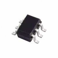
AD5612AKSZ-2REEL7 Analog Devices Inc, AD5612AKSZ-2REEL7 Datasheet - Page 17

AD5612AKSZ-2REEL7
Manufacturer Part Number
AD5612AKSZ-2REEL7
Description
IC,D/A CONVERTER,SINGLE,10-BIT,CMOS,TSSOP,6PIN
Manufacturer
Analog Devices Inc
Series
nanoDAC™r
Datasheet
1.AD5622AKSZ-2REEL7.pdf
(24 pages)
Specifications of AD5612AKSZ-2REEL7
Settling Time
6µs
Number Of Bits
10
Data Interface
I²C, Serial
Number Of Converters
1
Voltage Supply Source
Single Supply
Power Dissipation (max)
500µW
Operating Temperature
-40°C ~ 85°C
Mounting Type
Surface Mount
Package / Case
SC-70-6, SC-88, SOT-363
Lead Free Status / RoHS Status
Lead free / RoHS Compliant
POWER-ON RESET
The AD5602/AD5612/AD5622 each contain a power-on reset
circuit that controls the output voltage during power-up. The
DAC register is filled with zeros and the output voltage is 0 V
where it remains until a valid write sequence is made to the
DAC. This is useful in applications where it is important to
know the state of the DAC output while it is in the process of
powering up.
POWER-DOWN MODES
The AD5602/AD5612/AD5622 each contain four separate
modes of operation. These modes are software-programmable
by setting Bit PD1 and Bit PD0 in the control register. Table 7
shows how the state of the bits corresponds to the mode of
operation of the device.
Table 7. Modes of Operation
PD1
0
0
1
1
PD0
0
1
0
1
Operating Mode
Normal operation
Power-down (1 kΩ load to GND)
Power-down (100 kΩ load to GND)
Power-down (Three-state output)
Rev. B | Page 17 of 24
When both bits are set to 0, the part works normally with its
usual power consumption of 100 μA maximum at 5 V. However,
for the three power-down modes, the supply current falls to
<150 nA (at 3 V). Not only does the supply current fall, but the
output stage is internally switched from the output of the
amplifier to a resistor network of known values. This gives the
advantage of knowing the output impedance of the part while
the part is in power-down mode. There are three different
options. The output is connected internally to GND through a
1 kΩ resistor, a 100 kΩ resistor, or it is left open-circuited
(three-state). Figure 41 shows the output stage.
The bias generator, output amplifier, resistor string, and other
associated linear circuitry are all shut down when the power-
down mode is activated. However, the contents of the DAC
register are unaffected when in power-down. The time to exit
power-down is typically 14 μs for V
3 V (see Figure 28).
STRING DAC
RESISTOR
Figure 41. Output Stage During Power-Down
POWER-DOWN
AMPLIFIER
CIRCUITRY
AD5602/AD5612/AD5622
DD
= 5 V and 17 μs for V
RESISTOR
NETWORK
V
OUT
DD
=


