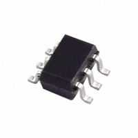
AD5612YKSZ-1REEL7 Analog Devices Inc, AD5612YKSZ-1REEL7 Datasheet - Page 16

AD5612YKSZ-1REEL7
Manufacturer Part Number
AD5612YKSZ-1REEL7
Description
IC,D/A CONVERTER,SINGLE,10-BIT,CMOS,TSSOP,6PIN
Manufacturer
Analog Devices Inc
Series
nanoDAC™r
Datasheet
1.AD5622AKSZ-2REEL7.pdf
(24 pages)
Specifications of AD5612YKSZ-1REEL7
Settling Time
6µs
Number Of Bits
10
Data Interface
I²C, Serial
Number Of Converters
1
Voltage Supply Source
Single Supply
Power Dissipation (max)
500µW
Operating Temperature
-40°C ~ 125°C
Mounting Type
Surface Mount
Package / Case
SC-70-6, SC-88, SOT-363
Lead Free Status / RoHS Status
Lead free / RoHS Compliant
AD5602/AD5612/AD5622
SERIAL INTERFACE
The AD5602/AD5612/AD5622 have 2-wire I
serial interfaces (refer to I
January 2000, available from Philips Semiconductor). The
AD5602/AD5612/AD5622 can be connected to an I
slave device, under the control of a master device. See Figure 2
for a timing diagram of a typical write sequence.
The AD5602/AD5612/AD5622 support standard (100 kHz),
fast (400 kHz), and high speed (3.4 MHz) data transfer modes.
Support is not provided for 10-bit addressing and general call
addressing.
The AD5602/AD5612/AD5622 each have a 7-bit slave address.
The five MSBs are 00011 and the two LSBs are determined by
the state of the ADDR pin. The facility to make hardwired
changes to ADDR allows the user to incorporate up to three of
these devices on one bus as outlined in Table 6.
The 2-wire serial bus protocol operates as follows:
1.
2.
The master initiates data transfer by establishing a start
condition, which is when a high-to-low transition on the
SDA line occurs while SCL is high. The following byte is
the address byte, which consists of the 7-bit slave address.
The slave address corresponding to the transmitted address
responds by pulling SDA low during the ninth clock pulse
(this is termed the acknowledge bit). At this stage, all other
devices on the bus remain idle while the selected device
waits for data to be written to, or read from, its shift register.
Data is transmitted over the serial bus in sequences of nine
clock pulses (eight data bits followed by an acknowledge
bit). The transitions on the SDA line must occur during the
low period of SCL and remain stable during the high
period of SCL.
DB15 (MSB)
DB15 (MSB)
DB15 (MSB)
0
0
0
2
C-Bus Specification, Version 2.1,
0
0
0
PD1
PD1
PD1
PD0
PD0
PD0
2
C-compatible
D11
D7
D9
Figure 38. AD5602 Input Register Contents
Figure 39. AD5612 Input Register Contents
Figure 40. AD5622 Input Register Contents
2
C bus as a
D10
D6
D8
D5
D7
D9
Rev. B | Page 16 of 24
DATA BITS
D4
D6
D8
DATA BITS
D3
D5
D7
3.
Table 6. Device Address Selection
ADDR
GND
V
NC (No Connection)
INPUT REGISTER
The input register is 16 bits wide. Figure 38, Figure 39, and
Figure 40 illustrate the contents of the input register for each
part. Data is loaded into the device as a 16-bit word under the
control of a serial clock input, SCL. The timing diagram for this
operation is shown in Figure 2. The 16-bit word consists of four
control bits followed by 8, 10, or 12 bits of data, depending on
the device type. MSB (DB15) is loaded first. The first two bits
are reserved bits that must be set to zero, the next two bits are
control bits that select the mode of operation of the device
(normal mode or any one of three power-down modes). See the
Power-Down Modes section for a complete description. The
remaining bits are left-justified DAC data bits, starting with the
MSB and ending with the LSB.
DD
DATA BITS
D2
D4
D6
When all data bits have been read or written, a stop
condition is established. In write mode, the master pulls
the SDA line high during the 10th clock pulse to establish a
stop condition. In read mode, the master issues a no
acknowledge for the ninth clock pulse (that is, the SDA line
remains high). The master then brings the SDA line low
before the 10th clock pulse, and then high during the 10th
clock pulse to establish a stop condition.
D1
D3
D5
D0
D2
D4
D1
D3
X
D0
D2
X
D1
A1
1
0
1
X
X
DB0 (LSB)
DB0 (LSB)
DB0 (LSB)
D0
X
X
A0
1
0
0


