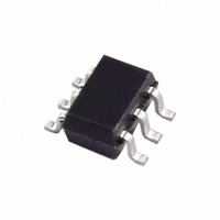
AD5612YKSZ-2REEL7 Analog Devices Inc, AD5612YKSZ-2REEL7 Datasheet - Page 7

AD5612YKSZ-2REEL7
Manufacturer Part Number
AD5612YKSZ-2REEL7
Description
IC,D/A CONVERTER,SINGLE,10-BIT,CMOS,TSSOP,6PIN
Manufacturer
Analog Devices Inc
Series
nanoDAC™r
Datasheet
1.AD5622AKSZ-2REEL7.pdf
(24 pages)
Specifications of AD5612YKSZ-2REEL7
Settling Time
6µs
Number Of Bits
10
Data Interface
I²C, Serial
Number Of Converters
1
Voltage Supply Source
Single Supply
Power Dissipation (max)
500µW
Operating Temperature
-40°C ~ 125°C
Mounting Type
Surface Mount
Package / Case
SC-70-6, SC-88, SOT-363
Lead Free Status / RoHS Status
Lead free / RoHS Compliant
PIN CONFIGURATION AND FUNCTION DESCRIPTIONS
Table 5. Pin Function Descriptions
Pin No.
1
2
3
4
5
6
ADDR
SCL
SDA
V
GND
V
Mnemonic
DD
OUT
Description
Three-State Address Input. Sets the two least significant bits (Bit A1, Bit A0) of the 7-bit slave address (see Table 6).
Serial Clock Line. This is used in conjunction with the SDA line to clock data into or out of the 16-bit input register.
Serial Data Line. This is used in conjunction with the SCL line to clock data into or out of the 16-bit input register. It
is a bidirectional, open-drain data line that should be pulled to the supply with an external pull-up resistor.
Power Supply Input. These parts can be operated from 2.7 V to 5.5 V, and V
Ground. The ground reference point for all circuitry on the part.
Analog Output Voltage from the DAC. The output amplifier has rail-to-rail operation.
ADDR
SDA
SCL
Figure 3. Pin Configuration
1
2
3
Rev. B | Page 7 of 24
(Not to Scale)
AD5602/
AD5612/
AD5622
TOP VIEW
6
5
4
V
GND
V
OUT
DD
DD
AD5602/AD5612/AD5622
should be decoupled to GND.


